Liquid crystal display panel and fabricating method thereof

Inactive Publication Date: 2008-03-06
CHUNGHWA PICTURE TUBES LTD
View PDF4 Cites 6 Cited by
  • Summary
  • Abstract
  • Description
  • Claims
  • Application Information

AI Technical Summary

Benefits of technology

[0010]Another objective of the present invention is to provide another liquid crystal display panel to eliminate the phenomena such as light leakage and dimness of the liquid crystal display panel, thereby maintaining the contrast of the liquid crystal display panel.
[0011]Still another object of the present invention is to provide a method of fabricating a liquid crystal display panel to eliminate the phenomena such as light leakage and dimness of the liquid crystal display panel, thereby maintaining the contrast and brilliance uniformity of the liquid crystal display panel.

Problems solved by technology

However, since conventional spacers are simply placed against between the two substrates, when the liquid crystal display panel is subjected to a lateral stress, the two substrates easily become mismatched with each other, thereby resulting in abnormal display phenomena such as light leakage and dimness.
This results in abnormal display phenomena of the liquid crystal display panel 100 such as light leakage and dimness.

Method used


Image

  • Liquid crystal display panel and fabricating method thereof
  • Liquid crystal display panel and fabricating method thereof
  • Liquid crystal display panel and fabricating method thereof

Examples


first embodiment

The First Embodiment

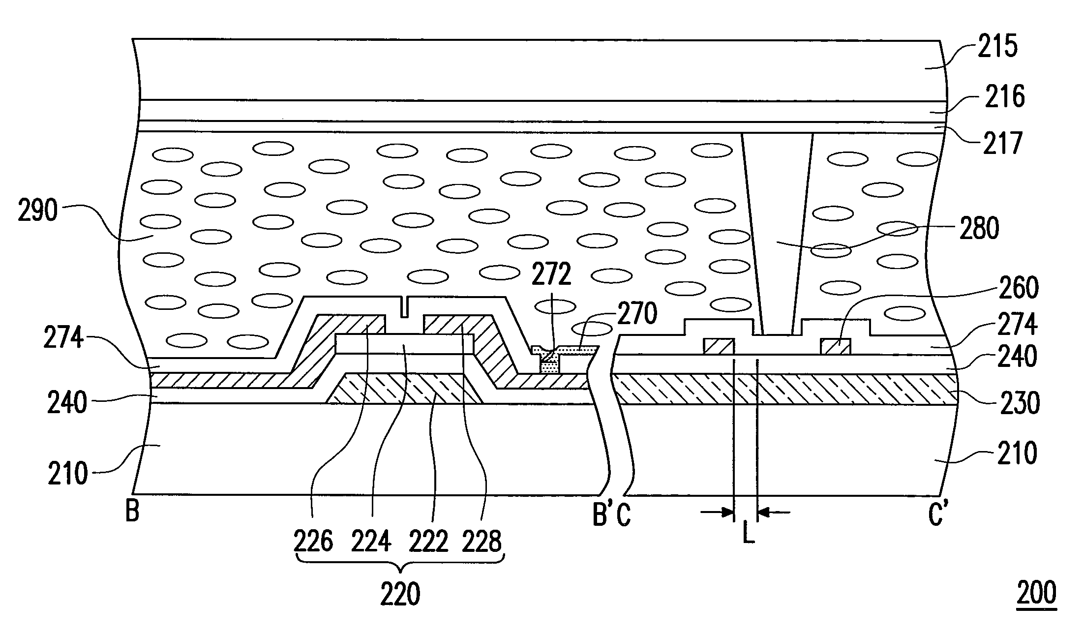
[0051]FIG. 3 is a schematic top view of one of the pixels of the TFT array substrate of the liquid crystal display panel according to one embodiment of the present invention. FIG. 4 is a sectional view of the liquid crystal display panel along Lines B-B′ and C-C′ in FIG. 3. Referring to FIGS. 3 and 4 together, the method of fabricating a liquid crystal display panel 200 comprises the steps as follows. First, a first substrate 210 is provided and a TFT process is performed on the first substrate 210. A plurality of gates 222 (only one gate is shown in the figures) and a plurality of scan lines 230 (only one scan line is shown in the figures) electrically connected to the gates 222 are formed on the first substrate 210. The forming method thereof comprises, for example, depositing a film layer and then performing an exposure process, a development process, and an etching process. After forming the gate 222 and the scan line 230, an insulation layer 240 is formed to...

second embodiment

The Second Embodiment

[0060]FIG. 7 is a sectional view of the liquid crystal display panel according to another embodiment of the present invention. Referring to FIG. 7, the embodiment is similar to the first embodiment except that the formed retaining wall pattern 264 is a structure having a lower layer 266 and an upper layer 268. The step of fabricating the liquid crystal display panel 200″ includes after the gate 222 and the insulation layer 240 are formed, the lower layer 266 of the retaining wall pattern 264 is formed when the channel layer 224 is formed on the insulation layer 240 over the gate 222. Therefore, the material of the lower layer 266 is the same as that of the channel layer 224. Then, the upper layer 268 of the retaining wall pattern 264 is formed when the source 226 and the drain 228 are formed on the channel layer 224. Therefore, the material of the upper layer 268 is the same as that of the source 226 and the drain 228. Similarly, the distance L between the pilla...

third embodiment

The Third Embodiment

[0062]FIG. 8 is a schematic sectional view of the liquid crystal display panel according to the third embodiment of the present invention. Referring to FIG. 8, the liquid crystal display panel 800 comprises a first substrate 810, a pixel array 820, and a color filter array 830. The pixel array 820 and the color filter array 830 are formed on the first substrate 810. Each pixel of the pixel array 820 comprises a scan line, a data line, a TFT, and a pixel electrode (not shown), and the pixel structure can be one of the conventional pixel structures. The color filter array 830 is disposed on the pixel array 820 and the pillar spacers 860 are disposed on the color filter array 830. Additionally, the second substrate 815 is disposed opposite to the first substrate 810 and the liquid crystal display panel 870 is disposed between the first substrate 810 and the second substrate 815. Particularly, a plurality of protrusions 840 are further formed on the second substrate ...


PUM


Abstract

A liquid crystal display panel includes a first substrate; a plurality of scan lines and a plurality of data lines disposed on the first substrate; an insulation layer disposed between the scan line and the data line; a plurality of thin film transistors (TFT), each TFT including a gate, a channel layer, a source, and a drain; a plurality of pixel electrodes; a plurality of retaining wall patterns disposed on the insulation layer and the material thereof is selected from at least one of the source / drain and channel layer; a second substrate disposed opposite to the first substrate; a liquid crystal layer between the first and second substrate; and a plurality of pillar spacers between the first and second substrate, wherein one end of the pillar spacer is disposed inside the retaining wall pattern.

Description

BACKGROUND OF THE INVENTION[0001]1. Field of Invention[0002]The present invention relates to a display panel and a fabricating method thereof. More particularly, the present invention relates to a liquid crystal display panel and a fabricating method thereof.[0003]2. Description of Related Art[0004]In modern society, multimedia technologies have been highly developed, benefiting from the progress of semiconductor devices or display units. As for displays, liquid crystal displays with the advantages of high quality picture, preferable space utilization, low power consumption, and no radiation, have gradually become mainstream products in the market.[0005]A liquid crystal display panel generally comprises two substrates and a liquid crystal layer sandwiched therebetween. In order to keep the height of the gap between the two substrates, multiple spacers are commonly disposed between the two substrates. However, since conventional spacers are simply placed against between the two subst...

Claims


Application Information

Patent Timeline
IPC IPC(8): G02F1/1339
CPCG02F1/13394G02F1/1362
Inventor WU, DER-CHUNLI, DE-JIUNCHIANG, HUNG-HSIANG
Owner CHUNGHWA PICTURE TUBES LTD
Why Eureka
Try Eureka