Light-emitting diode array, light-emitting diode, and printer head

a technology of light-emitting diodes and printer heads, which is applied in the direction of printing, electrical equipment, and semiconductor devices, can solve the problems of interfering with the degree of integration of light-emitting diodes, and achieve the effect of eliminating light leakage from corners

Inactive Publication Date: 2011-03-29
SANYO ELECTRIC CO LTD +1
View PDF18 Cites 5 Cited by
  • Summary
  • Abstract
  • Description
  • Claims
  • Application Information

AI Technical Summary

Benefits of technology

In the light-emitting diode array according to claim 1, in each of the plurality of platform-shaped light-emitting units formed so as to be isolated from each other, corners of the light-emitting units having a substantially square shape as viewed from above are provided with a beveled shape. Therefore, an electrode layer or light-blocking film can be wrapped around the corners when an electrode layer or light-blocking film is formed, enabling the corners to be covered by the electrode layer or light-blocking film and light leakage from the corners to be eliminated.
In the light-emitting diode array according to claim 2, the beveling of the corners is in an angle-beveled shape or a round-beveled shape, whereby the corners can be covered by an electrode layer or light-blocking film during formation of the electrode layer using a simple etching mask pattern, and light leakage from the corners can be eliminated.
In the light-emitting diode array according to claim 3, since an electrode layer or light-blocking film provided to each of the plurality of light-emitting units surrounds three sides as viewed from above of a light emitting window of each of the plurality of light-emitting units and extends to the mesa surfaces and a base at the bottom of the mesa surfaces, light is prevented from emanating from the forward mesa surfaces, the beveled portion at the corners, and the upper surface other than the area of the light emitting window. Light can also be prevented from leaking from the forward mesa surfaces, the corner portions, and the upper surface other than the area of the light emitting window of the light-emitting diode.
The light-emitting diode according to claim 4 has a light-emitting unit in which an electrode is formed on each surface tilted outward from top to bottom of a pair of opposing side surfaces among four peripheral side surfaces, and an electrode is also formed in wraparound fashion near corners of each surface tilted inward from top to bottom of the pair of opposing side surfaces adjacent to the pair of opposing side surfaces, so as to connect to the electrode provided to each surface tilted outward from top to bottom of the pair of opposing side surfaces. Therefore, in this light-emitting diode, the upper surface, each of a pair of opposing side surfaces, and the areas near the corners of each of the pair of opposing side surfaces adjacent to the pair of opposing side surfaces can be covered by the electrode, and light can be prevented from leaking from these surfaces.
A configuration is adopted whereby the shape of the corners of the light-emitting unit can be selected according to the shape of an etching mask pattern in the light-emitting diode array or light-emitting diode according to the present invention. There is therefore no need to add more steps to the conventional fabrication process, and it is possible to freely select a corner shape for the light-emitting diode that is optimal for the conditions of the manufacturing process.

Problems solved by technology

This light leakage significantly interferes with enhancing the degree of integration of the light-emitting diodes.

Method used


Image

  • Light-emitting diode array, light-emitting diode, and printer head
  • Light-emitting diode array, light-emitting diode, and printer head
  • Light-emitting diode array, light-emitting diode, and printer head

Examples


Embodiment Construction

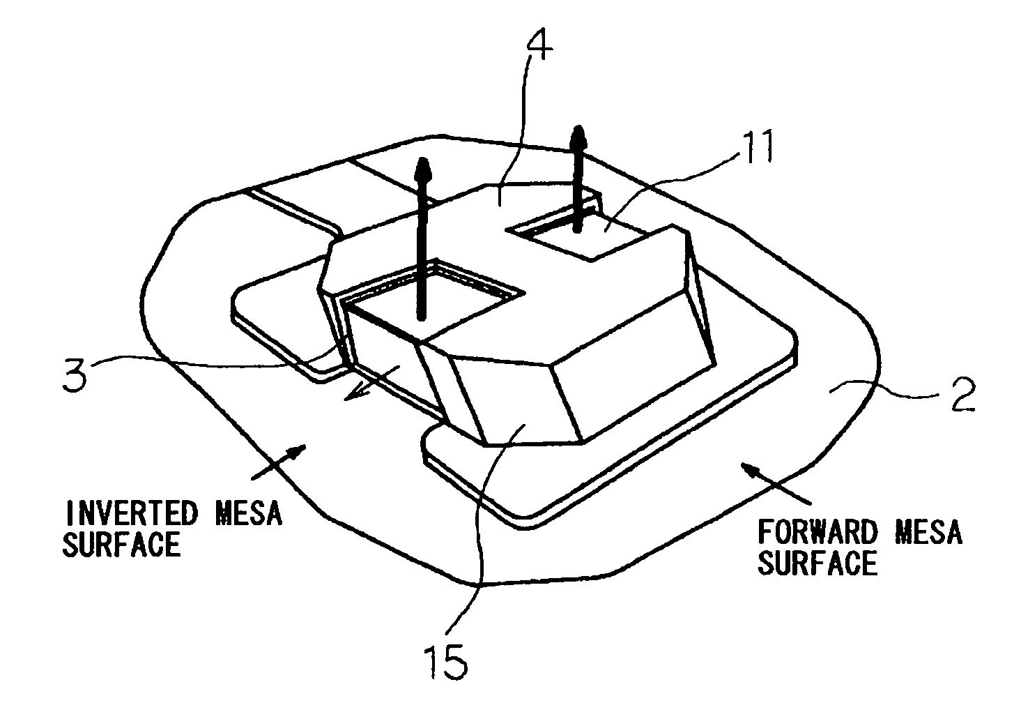
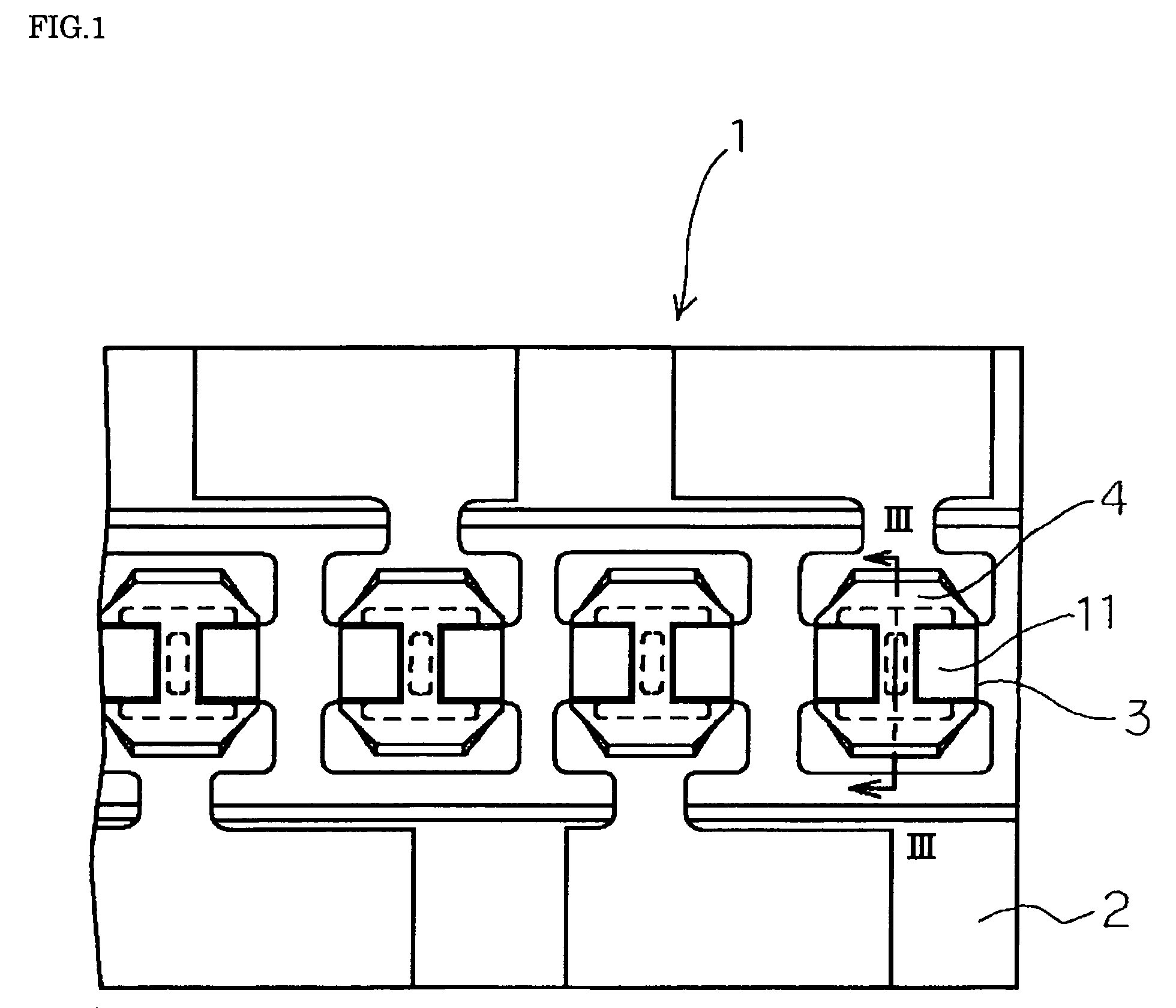
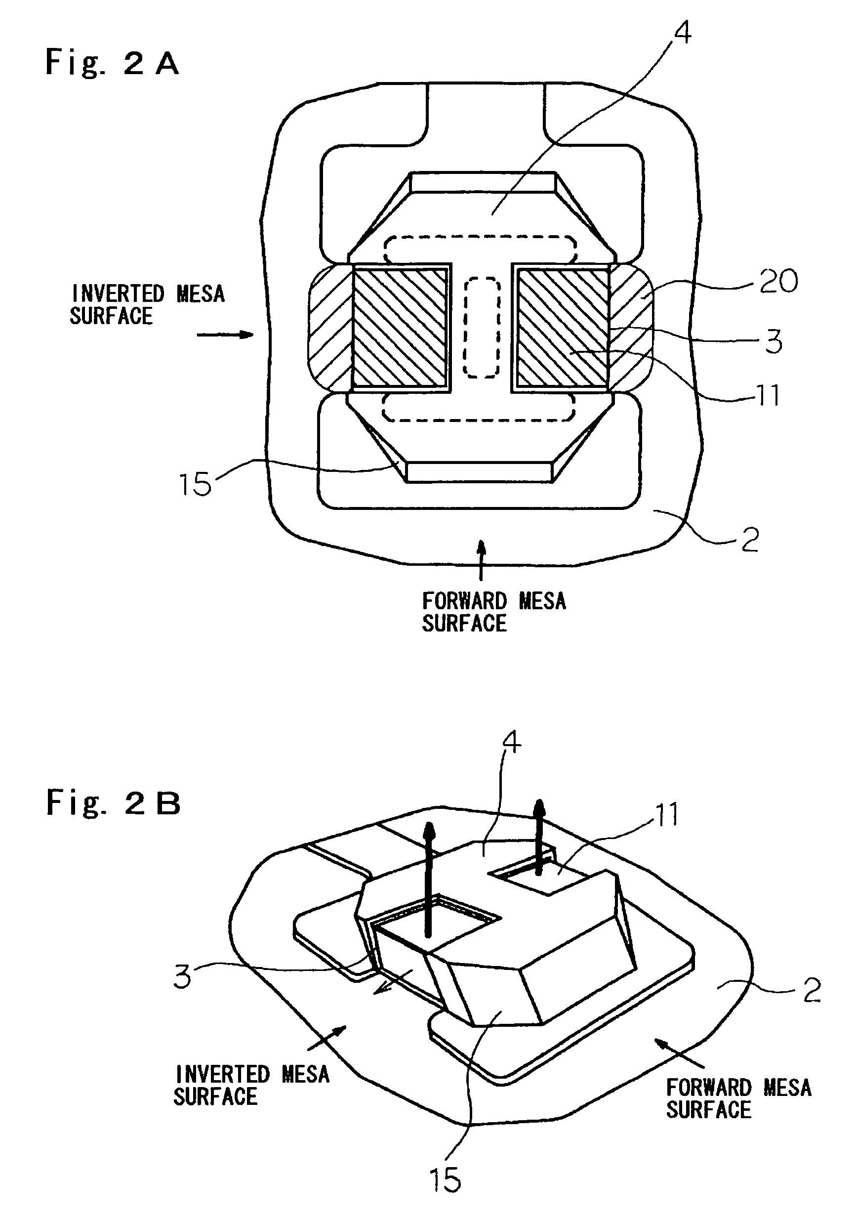
Examples of the light-emitting diode array according to the present invention will be described in detail hereinafter with reference to the drawings. FIG. 1 is a schematic top view of an example of the light-emitting diode array according to the present invention. This light-emitting diode array 1 is composed of a base 2 that includes a substrate, an N-electrode layer, a buffer layer, a distributed Bragg reflector layer, and an insulating film; a plurality of platform-shaped light-emitting units 3 formed in the upper surface portion by, for example, mesa etching so as to be isolated from each other; and P-electrode layers 4.

The shape of each of the plurality of light-emitting units 3 is such that the light-emitting units having a substantially square shape as viewed from above are provided with beveled corners. Light emitting windows 11 in two positions of the light-emitting units 3 are disposed adjacent to each other at a prescribed interval in the transverse direction.

P-electrode ...


PUM


Abstract

A light emitting diode array in which, when viewed from the above, the shape of an almost square light emitting diode is square-chamfered or round-chamfered at the corners thereof in order to minimize light leakage at a reverse mesa surface to allow an electrode layer to surround the three directions of a light emitting unit, and part in the vicinity of the corner of the reverse mesa surface is extended up to a substrate unit to cover it. Accordingly, the light emitting diode array minimized in light leakage at the reverse mesa surface can be provided.

Description

TECHNICAL FIELDThe present invention relates to a light-emitting diode array and light-emitting diode used in a printer head or other components of an LED (light-emitting diode) printer, and particularly relates to a mesa-isolated monolithic light-emitting diode array, to a light-emitting diode, and to a printer head.BACKGROUND ARTPrinters have recently come to be used in a wider range of applications that is not limited to text and graphics, but also extends to photographic printing, and progressively higher levels of detail and clearly discernable printing are desired.Enhanced printing precision is also desired in a light-emitting diode array used in the printer head of an LED printer, and techniques are being developed to meet the need for micro-fabrication and increased luminance of such light-emitting diode arrays.However, the area of the light-emitting surface increases as a result of light leakage from the light-emitting portions of each of the plurality of light-emitting dio...

Claims


Application Information

Patent Timeline
Patent Type & Authority Patents(United States)
IPC IPC(8): H01L33/00B41J2/44B41J2/45B41J2/455H01L33/20H01L33/38
CPCB41J2/45H01L33/20H01L33/385H01L25/0753H01L2924/0002
Inventor YAMAMOTO, HIRONORIKIMACHI, HAJIME
Owner SANYO ELECTRIC CO LTD
Why Eureka
Try Eureka