Liquid crystal display panel

a liquid crystal display and display panel technology, applied in non-linear optics, instruments, optics, etc., can solve the problems of sacrificing the light transmission area the edge of data lines and the pixel display area of the display panel, and the existence of light leakage, so as to reduce the size of the black matrix and even eliminate the effect of the aperture ratio of the pixel uni

Inactive Publication Date: 2015-07-09
TCL CHINA STAR OPTOELECTRONICS TECH CO LTD
View PDF2 Cites 6 Cited by
  • Summary
  • Abstract
  • Description
  • Claims
  • Application Information

AI Technical Summary

Benefits of technology

[0023]Compared with the prior art, the beneficial effects of the present disclosure is in that, in each pixel area on the array substrate, the shielding electrode covers onto electric conductors (such as the data line and the scan line) having different potentials from the pixel electrode to prevent electric fields from being formed between the electric conductors and the common electrode line, so that light leakage in the pixel units due to liquid crystal electrons being subjected to disordered electric fields may be reduced. Further, because the shielding electrode of each pixel unit covers onto the data line and the scan line, the black matrix may be reduced in size and even eliminated. In this way, with light leakage eliminated, the aperture ratio of the pixel units may be improved at the same time.

Problems solved by technology

Due to these, the brightness at the edge of scan lines, the edge of data lines and the pixel display areas of the display panel are inconsistent, namely light leakage exists.
Moreover, to prevent light leakage caused by deflection of two glass sheets (the array substrate and the color filter substrate) of the liquid crystal display panel due to processing errors or external force, the black matrix is arranged to cover and exceed the data lines and the scan lines for a certain distance in design, which is bound to sacrifice the light transmission area of the pixel units, namely the aperture ratio of the pixel units is declined, so that rise of energy consumption of the whole display panel is indirectly caused.

Method used


Image

  • Liquid crystal display panel
  • Liquid crystal display panel
  • Liquid crystal display panel

Examples


Embodiment Construction

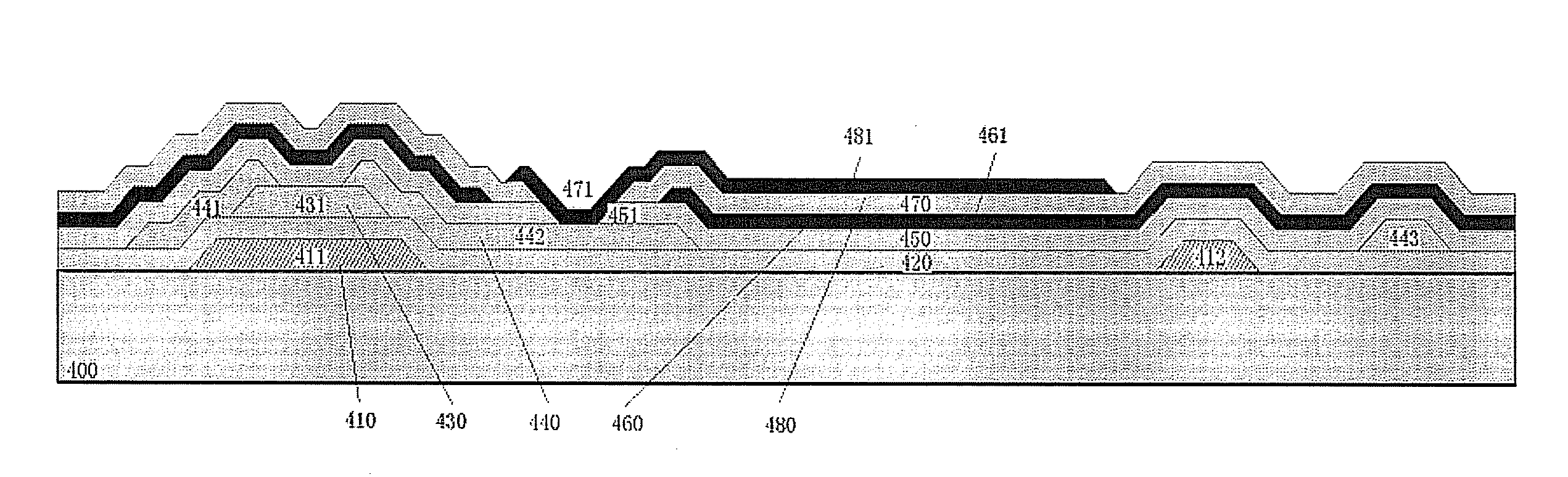
[0035]In a pixel unit of a liquid crystal display panel proposed in the present disclosure, a layer of shielding electrode covers onto a data line and a scan line which are electrically connected with said pixel unit and onto other electric conductors having different potentials from a pixel electrode of said pixel unit, to shield the data line, the scan line and a power line from the electric conductor to a common electrode. In this way, light leakage is reduced. Moreover, as a result of the shielding electrode, a black matrix may be reduced in size and even completely eliminated. By mean of these, with light leakage reduced, the aperture ratio of the pixel units is improved at the same time, thus reducing the energy consumption of the whole display device.

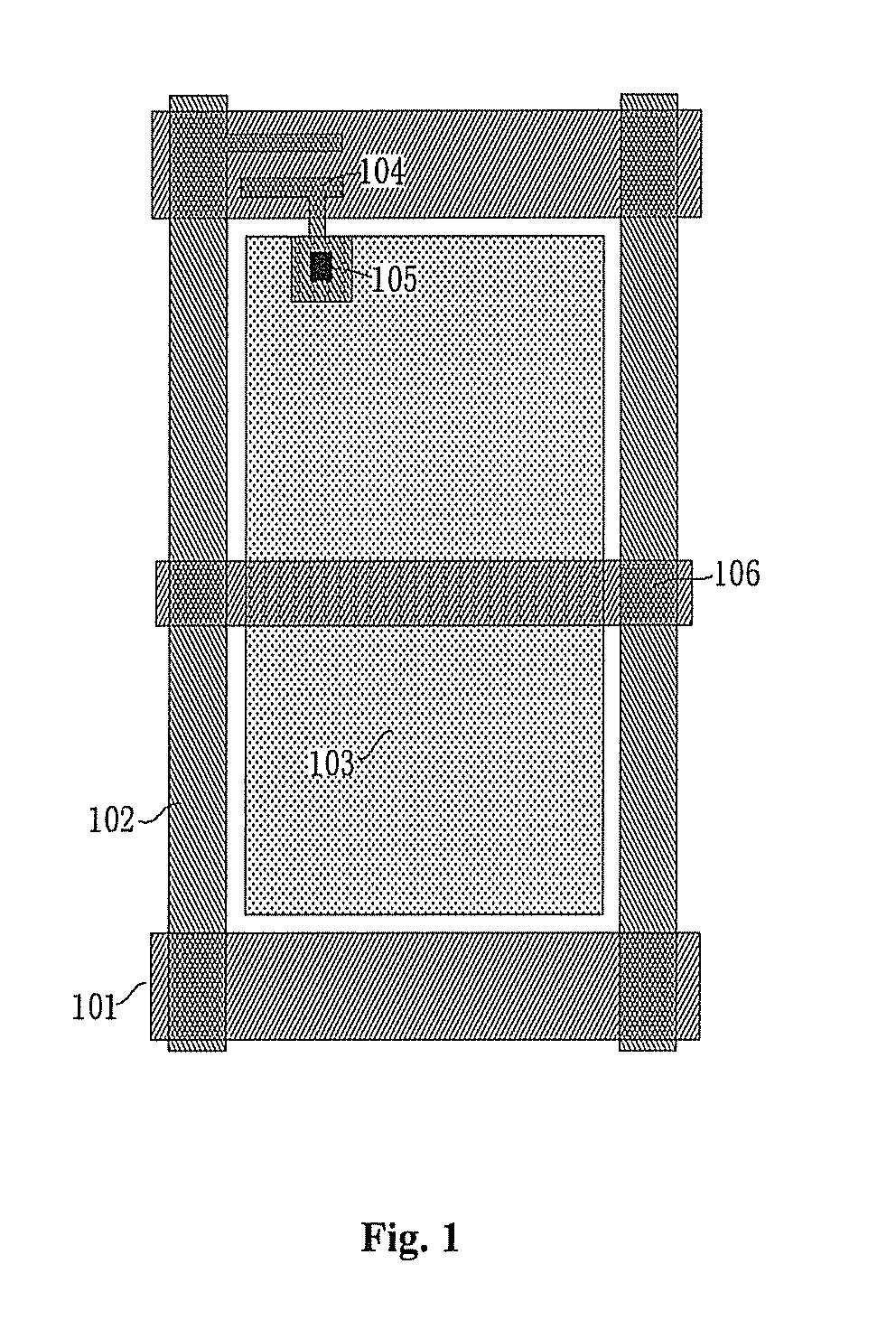
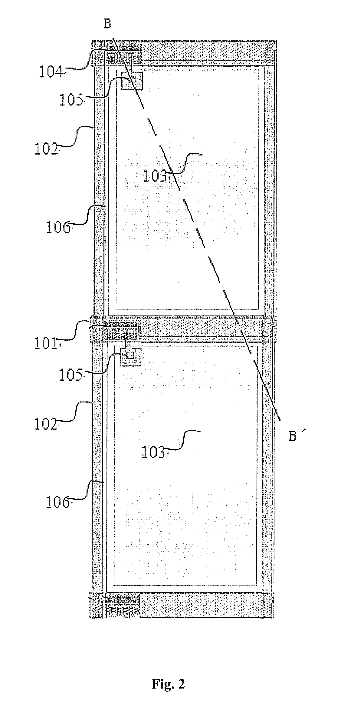
[0036]As shown in FIG. 2 and FIG. 3, specifically, in above-mentioned pixel unit of the liquid crystal display panel, said shielding electrode may be electrically connected to the common electrode to have a potential of the commo...


PUM

PropertyMeasurementUnit
areaaaaaaaaaaa
transparentaaaaaaaaaa
non-transparent conductiveaaaaaaaaaa

Abstract

The present disclosure relates to a liquid crystal display panel including an array substrate, the array substrate comprising: a substrate; a plurality of common electrode lines arranged on the substrate; a plurality of scan lines and data lines arranged on the substrate in a staggered manner to form a plurality of pixel areas; and a plurality of pixel units, each of which is arranged in a pixel area and includes a pixel electrode and a switching element, wherein the switching element is electrically connected to the scan line, the data line and the pixel electrode and is turned on under the action of a voltage signal of the scan line to transmit a voltage signal on the data line to the pixel electrode, so that the pixel electrode has a corresponding potential; and wherein in each pixel area, a shielding electrode electrically connected to the pixel electrode or the common electrode line covers the above of the scan line and the data line. The liquid crystal display panel of the present invention can reduce a phenomenon of light leakage and further have an improved aperture ratio of the pixel units.

Description

FIELD OF THE INVENTION[0001]The present disclosure relates to the technical field of liquid crystal display, and particularly relates to a liquid crystal display panel for reducing light leakage.BACKGROUND OF THE INVENTION[0002]An active thin film transistor liquid crystal display (TFT LCD) panel has become a mainstream product on the market with its excellent performance. One active TFT LCD panel generally consists of an array substrate, a color filter substrate and a liquid crystal layer. Wherein, a plurality of scan lines and data lines are arranged on the array substrate in a staggered manner to form a plurality of pixel areas, and one pixel unit is configured in each pixel area. Each pixel unit at least includes a thin film transistor (TFT) and a pixel electrode correspondingly connected with the TFT. The TFT, as a switching element for starting the pixel unit to operate, is connected to a scan line and a data line and thereby loads the voltage of a data signal to the correspon...

Claims


Application Information

Patent Timeline
Patent Type & Authority Applications(United States)
IPC IPC(8): G02F1/1362G02F1/1333G02F1/1343G02F1/1368
CPCG02F1/136209G02F1/1368G02F1/136286G02F2001/136218G02F1/133345G02F1/13439G02F2001/136222G02F1/136227G02F1/134309G02F2201/40G02F1/136218G02F1/136222
Inventor LIAO, ZUOMIN
Owner TCL CHINA STAR OPTOELECTRONICS TECH CO LTD
Why Eureka
Try Eureka