

Thin film diode and cascaded structure thereof
A thin-film diode and series structure technology, which is applied in the direction of electrical components, electric solid devices, circuits, etc., can solve the problems of forward bias resistance and reverse leakage current suppression structure complex, so as to improve the suppression effect, reduce leakage current, The effect of simplifying the functional structure
- Summary
- Abstract
- Description
- Claims
- Application Information
AI Technical Summary
Problems solved by technology
Method used
Image

Examples
Embodiment 1
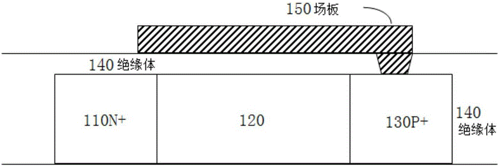
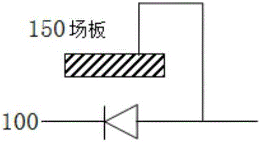
[0049] see figure 1 and figure 2 A thin film diode provided in this embodiment includes: a thin film diode body 100 and a field plate 150 located outside the low-doped drift region 120 of the thin film diode body; an insulator 140 is provided between the field plate 150 and the thin film diode body 100 .
[0050] Specifically, the field plate 150 is connected to the anode 130 of the thin film diode body; forming a forward bias resistor and a reverse leakage current suppression circuit structure.
[0051]Wherein, in a forward bias state, the positive power applied to the anode 130 biases the field plate 150 ; thereby suppressing the forward bias resistance. In the reverse bias state, a negative voltage applied to the cathode 110 biases the field plate 150; thereby suppressing reverse leakage current. That is, the control source of the field plate 150 is set to the thin film diode body 100, and its suppression operation is consistent with the state of the thin film diode body...
Embodiment 2
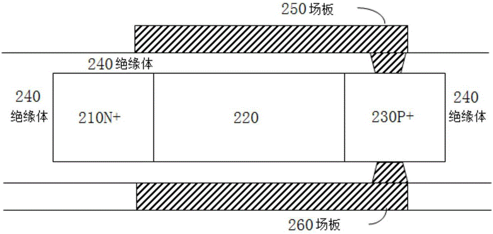
[0054] see image 3 , on the basis of Embodiment 1, this embodiment makes a design for the arrangement structure of the field plate.
[0055] Specifically, the field plate includes: a first field plate 250 and a second field plate 260 located on the upper and lower sides of the low-doped drift region 220 of the thin film diode body.
[0056] Wherein, the first field plate 250 and the second field plate 260 are respectively connected to the anode 230 of the thin film diode body. An insulator 240 is disposed between the first field plate 250 , the second field plate 260 and the thin film diode body.
[0057] In the forward bias state, the positive power applied to the anode 230 biases the first field plate 250 and the second field plate 260; in the reverse bias state, the negative voltage applied to the cathode 210 biases The first field plate 250 and the second field plate 260 . The suppression effect of forward bias resistance and directional leakage current is further enha...
Embodiment 3
[0059] see Figure 4 and Figure 5 , on the basis of the second embodiment, the structure of the first field plate is changed.
[0060] Specifically, the first field plate 350 includes: a top field plate located on the top side of the low-doped drift region of the thin film diode body 300 and side field plates located on the left and right sides of the low-doped drift region of the thin film diode body ; That is, the first field plate 350 is arranged in a C-shaped structure, buckled on the thin film diode body 300 , and an insulator 340 is arranged between them.
[0061] The side field plate is connected to the top field plate and connected to the anode 330 of the thin film diode body 300 .
[0062] Wherein, in the forward bias state, the positive power applied to the anode 330 biases the top field plate, the side field plate and the second field plate 360; in the reverse bias state, the positive power applied to The negative voltage at cathode 310 biases the top field plat...
PUM
 Abstract
Description
Claims
Application Information