Method for implementing single point grounding design, single-point grounding PCB package and printed circuit board

A printed circuit board, single-point grounding technology, applied in the field of electronics, to achieve the effect of easy to modify the layout, reduce workload, achieve standardized design and automated processing

Active Publication Date: 2017-05-31
QIKU INTERNET TECH SHENZHEN CO LTD
View PDF3 Cites 4 Cited by
  • Summary
  • Abstract
  • Description
  • Claims
  • Application Information

AI Technical Summary

Problems solved by technology

[0010] The main purpose of the present invention is to provide a method for realizing single-point grounding design, single-point grounding PCB package and printed circuit board, aiming to solve the above-mentioned technical problems that occur when performing single-point grounding design through manual control

Method used


Image

  • Method for implementing single point grounding design, single-point grounding PCB package and printed circuit board
  • Method for implementing single point grounding design, single-point grounding PCB package and printed circuit board
  • Method for implementing single point grounding design, single-point grounding PCB package and printed circuit board

Examples


Embodiment Construction

[0046] It should be understood that the specific embodiments described here are only used to explain the present invention, not to limit the present invention.

[0047] Embodiments of the present invention are described in detail below, examples of which are shown in the drawings, wherein the same or similar reference numerals designate the same or similar elements or elements having the same or similar functions throughout. The embodiments described below by referring to the figures are exemplary only for explaining the present invention and should not be construed as limiting the present invention.

[0048] Those skilled in the art will understand that unless otherwise stated, the singular forms "a", "an", "said" and "the" used herein may also include plural forms. It should be further understood that the word "comprising" used in the description of the present invention refers to the presence of said features, integers, steps, operations, elements and / or components, but does ...


PUM


Abstract

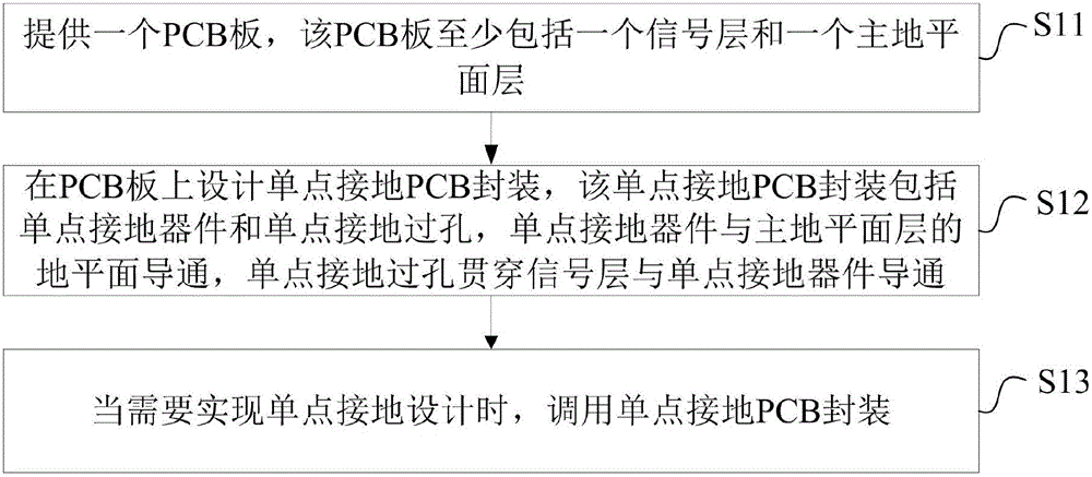
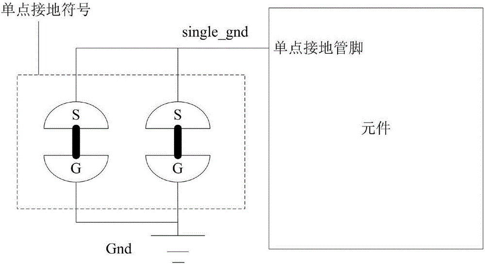
The invention discloses a method for implementing a single point grounding design, a single point grounding PCB package and a printed circuit board. The method comprises the steps that a PCB is provided and at least comprises a signal layer and a main horizontal layer; the single-point grounding PCB package is designed on the PCB, including a single-point grounding device and a single-point grounding vent hole; the single-point grounding device is arranged on the main horizontal layer, and is communicated with the horizon of the main horizontal layer; the single-point grounding vent hole runs through the signal layer, is communicated with the single-point grounding device, and is isolated from the signal region in the signal layer; and the single-point grounding PCB package is called when single-point grounding design is required to implement. Therefore, single-point grounding is used as an independent device for processing, and the device is provided with graphic symbols corresponding to a schematic circuit diagram and a package structure corresponding to PCB, so that standard design and automatic processing of single-point grounding can be realized, and the design efficiency and reliability of PCB can be improved.

Description

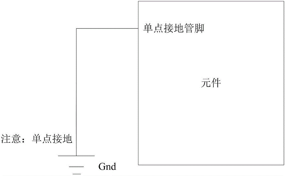
technical field [0001] The invention relates to the field of electronic technology, in particular to a method for realizing a single-point grounding design, a single-point grounding PCB package and a printed circuit board. Background technique [0002] As more and more functions are integrated in the design of various electronic products, there are more and more designs for integrating baseband, radio frequency, audio, power management and other module circuits on a printed circuit board (PCB). In these module circuits, most of the baseband circuits are digital circuits; while most of the circuits such as radio frequency, audio frequency, and power management involve analog circuits. In the design scheme with both digital circuits and analog circuits, it is usually necessary to use single-point grounding for low-frequency circuits such as analog and audio, that is, to connect the ground wires of each circuit module to the main ground plane at a certain point. . [0003] Th...

Claims


Application Information

Patent Timeline
Patent Type & Authority Applications(China)
IPC IPC(8): H05K1/02
Inventor 李帅
Owner QIKU INTERNET TECH SHENZHEN CO LTD
Why Eureka
Try Eureka