
Wafer lapping equipment with dust collection function

A chip and equipment technology, applied in the field of optoelectronic information, can solve the problems of low processing efficiency, long processing time, easy edge collapse of the chip edge, etc., to achieve energy saving, lubricate equipment and heat dissipation, and avoid flying dust.

Active Publication Date: 2017-06-13
重庆晶宇光电科技有限公司
View PDF7 Cites 8 Cited by
  • Summary
  • Abstract
  • Description
  • Claims
  • Application Information

AI Technical Summary

Problems solved by technology

[0002] Wafers processed by traditional wafer grinding equipment generally have the problem that the edge of the wafer is easy to sag
The reason for this problem is that the regular grinding path causes the edge wear to be greater than that of the inside and is easy to form sagging. The qualified rate of the finished product obtained by the original wafer grinding device is low, the processing time is long, resulting in low processing efficiency and high cost, and the surface is rough. Indexes such as degree of flatness, flatness, and wafer thickness tolerance cannot meet the requirements for processing patterned substrate wafers
[0003] With the rapid development of optoelectronic technology, optoelectronic products require a large number of wafers. In order to meet the needs of the development of optical devices, a variety of grinding devices with high work efficiency, low scrap rate, high product smoothness, and low cost have appeared on the market. However, these grinding During the processing of the device, a lot of powder chips will be generated, and the powder chips will fly everywhere, which is not easy to clean, and the power equipment used for grinding is prone to rust and aging after long-term operation. It is very troublesome to lubricate, maintain and clean the power equipment regularly.

Method used


Image

  • Wafer lapping equipment with dust collection function
  • Wafer lapping equipment with dust collection function

Examples


Embodiment Construction

[0017] The present invention will be described in further detail below by means of specific embodiments:

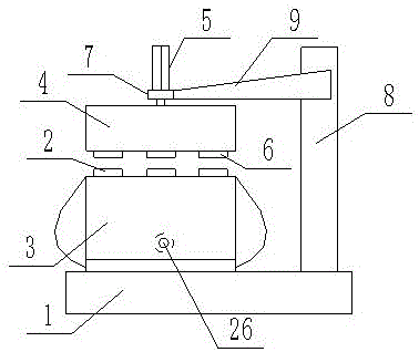
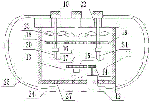
[0018] The reference signs in the accompanying drawings of the specification include: a base 1, a wafer holder 2, a workbench 3, a grinding mechanism 4, a pressurizing mechanism 5, a grinding head 6, a connector 7, a movable support 8, a support arm 9, and a wafer 10 , the first driving mechanism 11, the motor 12, the transmission structure 13, the output gear 14, the speed regulating gear 15, the driven gear 16, the rotating shaft 17, the second driven gear 18, the third driven gear 19, the second rotating shaft 20, The third rotating shaft 21 , the first through hole 22 , the fan blade 23 , the oil tank 24 , the oil delivery pipe 25 , the second driving mechanism 26 , and the second through hole 27 .

[0019] This embodiment is basically as figure 1 Shown:

[0020] Wafer grinding equipment with a dust suction function, including a base 1 for supporting the grinding eq...


PUM


Abstract

The invention relates to the technical field of photoelectronic information, and discloses wafer lapping equipment with a dust collection function. The wafer lapping equipment comprises a base platform, wafer carrying bosses, a working table, a lapping mechanism and a pressurizing mechanism, wherein a first driving mechanism is arranged in the working table; the first driving mechanism comprises a motor and a transmission structure; first through holes communicating with the inside of the working table are formed in the surface of the working table; rotating shafts of the transmission mechanism penetrate through the through holes and are used for supporting the wafer carrying bosses; fan blades are arranged on the rotating shafts between the wafer carrying bosses and a driven gear; an oil tank is connected below the working table; second through holes communicating with the oil tank are formed in the bottom of the working table; the oil tank is connected with oil conveying pipes; and oil outlets of the oil conveying pipes are located at two of the first through holes. The invention aims to provide the wafer lapping equipment with the dust collection function; in a process of lapping wafers, dust generated by lapping can be collected, and heat dissipation and lubrication effects can be achieved on the equipment.

Description

technical field [0001] The invention relates to the field of optoelectronic information technology, in particular to a wafer grinding device with dust suction function. Background technique [0002] Wafers processed by traditional wafer grinding devices generally have the problem that the edge of the wafer is easy to sag. The reason for this problem is that the regular grinding path causes the edge wear to be greater than that of the inside and is easy to form sag. The qualified rate of the finished product obtained by the original wafer grinding device is low, and the processing time is long, resulting in low processing efficiency and high cost, and the surface is rough. Degree, flatness, wafer thickness tolerance and other indicators cannot meet the requirements for processing patterned substrate wafers. [0003] With the rapid development of optoelectronic technology, optoelectronic products require a large number of wafers. In order to meet the needs of the development ...

Claims


Application Information

Patent Timeline
Patent Type & Authority Applications(China)
IPC IPC(8): B24B37/10B24B37/30B24B37/34B24B55/06
CPCB24B37/105B24B37/30B24B37/34B24B55/06
Inventor 侯明永
Owner 重庆晶宇光电科技有限公司
Learn More