Check patentability & draft patents in minutes with Patsnap Eureka AI!

CVD film and its etching treatment method

A processing method and thin film technology, applied in the preparation of test samples, etc., can solve the problems of time-consuming test, long test cycle, difficult monitoring, high wet etching uniformity, etc.

Active Publication Date: 2020-10-23
TRULY HUIZHOU SMART DISPLAY
View PDF5 Cites 0 Cited by
  • Summary
  • Abstract
  • Description
  • Claims
  • Application Information

AI Technical Summary

Problems solved by technology

[0003] One method is to make a pattern of the sample to be tested by photolithography, dry etching and stripping process, and use a step meter to test the step difference between the patterns, so as to reflect the amount of etching and calculate the etching rate; The method requires multiple positions to cooperate with the test, the test is time-consuming, and the generally set test cycle is long, making it difficult to monitor
[0004] Another method is to use wet etching to etch the film layer under the condition of incomplete etching after testing the film thickness with an ellipsometer in advance, then test the film thickness again, and compare the difference between the two to give The result; this method has high requirements on the uniformity of wet etching, and the data of film quality uniformity cannot be obtained, and it also requires the cooperation of other posts
[0005] It can be seen that the existing film etching rate test method needs to make the CVD film circulate in multiple positions when etching the CVD film, which is not conducive to industrial production.

Method used


Image

  • CVD film and its etching treatment method
  • CVD film and its etching treatment method
  • CVD film and its etching treatment method

Examples


Embodiment Construction

[0044] In order to make the object, technical solution and advantages of the present invention clearer, the present invention will be further described in detail below in conjunction with the accompanying drawings and embodiments. It should be understood that the specific embodiments described here are only used to explain the present invention, not to limit the present invention.

[0045] In the description of the present invention, it should be understood that the terms "first" and "second" are used for description purposes only, and cannot be interpreted as indicating or implying relative importance or implicitly indicating the quantity of indicated technical features. Thus, the features defined as "first" and "second" may explicitly or implicitly include at least one of these features. In the description of the present invention, "plurality" means at least two, such as two, three, etc., unless otherwise specifically defined.

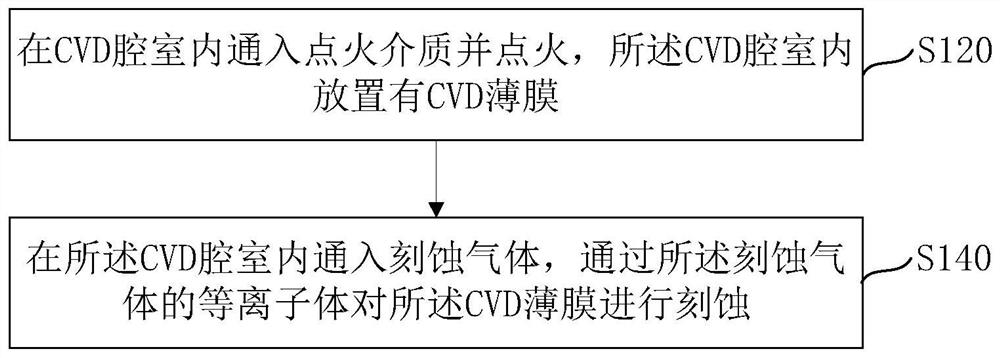
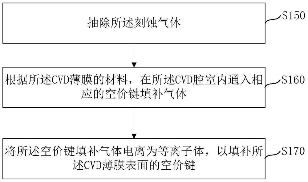
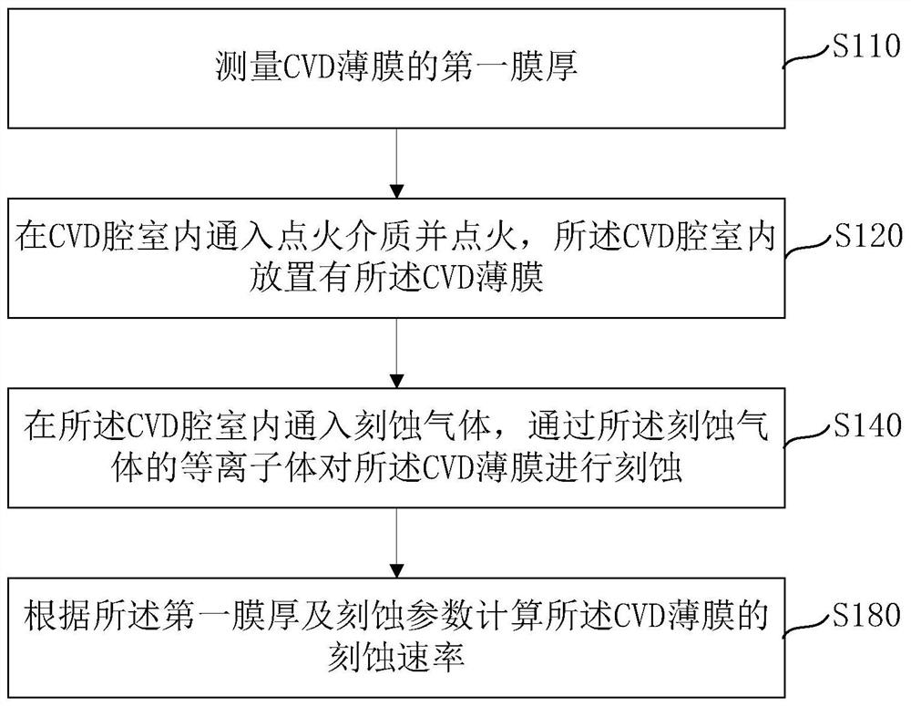
[0046] For example, the etching treatment met...


PUM


Abstract

The invention provides a CVD (Chemical Vapor Deposition) thin film and an etching treatment method thereof. The etching treatment method comprises the steps of feeding an ignition medium in a CVD cavity, wherein the CVD thin film is placed in the CVD cavity; feeding an etching gas into the CVD cavity, and etching the CVD thin film through a plasma of the etching gas. According to the CVD thin film and the etching treatment method thereof, the etching gas is fed into the CVD cavity so as to etch the CVD thin film, so that the thin film is formed and etched through a CVD device, the circulation times of the product between different stations is reduced, and the production efficiency can be improved.

Description

technical field [0001] The invention relates to the field of display technology, in particular to a CVD thin film and an etching treatment method thereof. Background technique [0002] Currently, PECVD (Plasma Enhanced Chemical Vapor Deposition, Plasma Enhanced Chemical Vapor Deposition) is an indispensable film forming process in the manufacturing process of display devices such as TFT (Thin film transistor, thin film transistor). In the industrial production process, it is necessary to detect the quality of the film formed by CVD, so as to find the quality problems of the product in time and adjust the process parameters. Among them, in addition to film thickness, refractive index, and film formation rate, the etching rate of the film is also one of the criteria for judging whether the film is qualified. At present, there are two main methods for testing the etching rate: [0003] One method is to make a pattern of the sample to be tested by photolithography, dry etching...

Claims


Application Information

Patent Timeline
Patent Type & Authority Patents(China)
IPC IPC(8): G01N1/32
CPCG01N1/32
Inventor 李松举李成祝汉泉苏君海李建华
Owner TRULY HUIZHOU SMART DISPLAY
Features
  • R&D
  • Intellectual Property
  • Life Sciences
  • Materials
  • Tech Scout
  • Unparalleled Data Quality
  • Higher Quality Content
  • 60% Fewer Hallucinations
Learn More