PCB (Printed Circuit Board) dual-frequency communication antenna

A communication antenna and PCB board technology, applied in the field of antennas, can solve the problems of difficult processing, high cost, low integration, etc., and achieve the effects of good gain flatness and easy antenna processing

Pending Publication Date: 2017-06-13
ALLWIN TELECOMM
View PDF5 Cites 4 Cited by
  • Summary
  • Abstract
  • Description
  • Claims
  • Application Information

AI Technical Summary

Problems solved by technology

[0004] At present, antennas for ISM application communication systems such as Wifi and Zigbee on the market have large working volume, difficult processing, and high cost, and 2.4G and 5.8G are generally designed separately, with low integration

Method used


Image

  • PCB (Printed Circuit Board) dual-frequency communication antenna
  • PCB (Printed Circuit Board) dual-frequency communication antenna
  • PCB (Printed Circuit Board) dual-frequency communication antenna

Examples


Embodiment

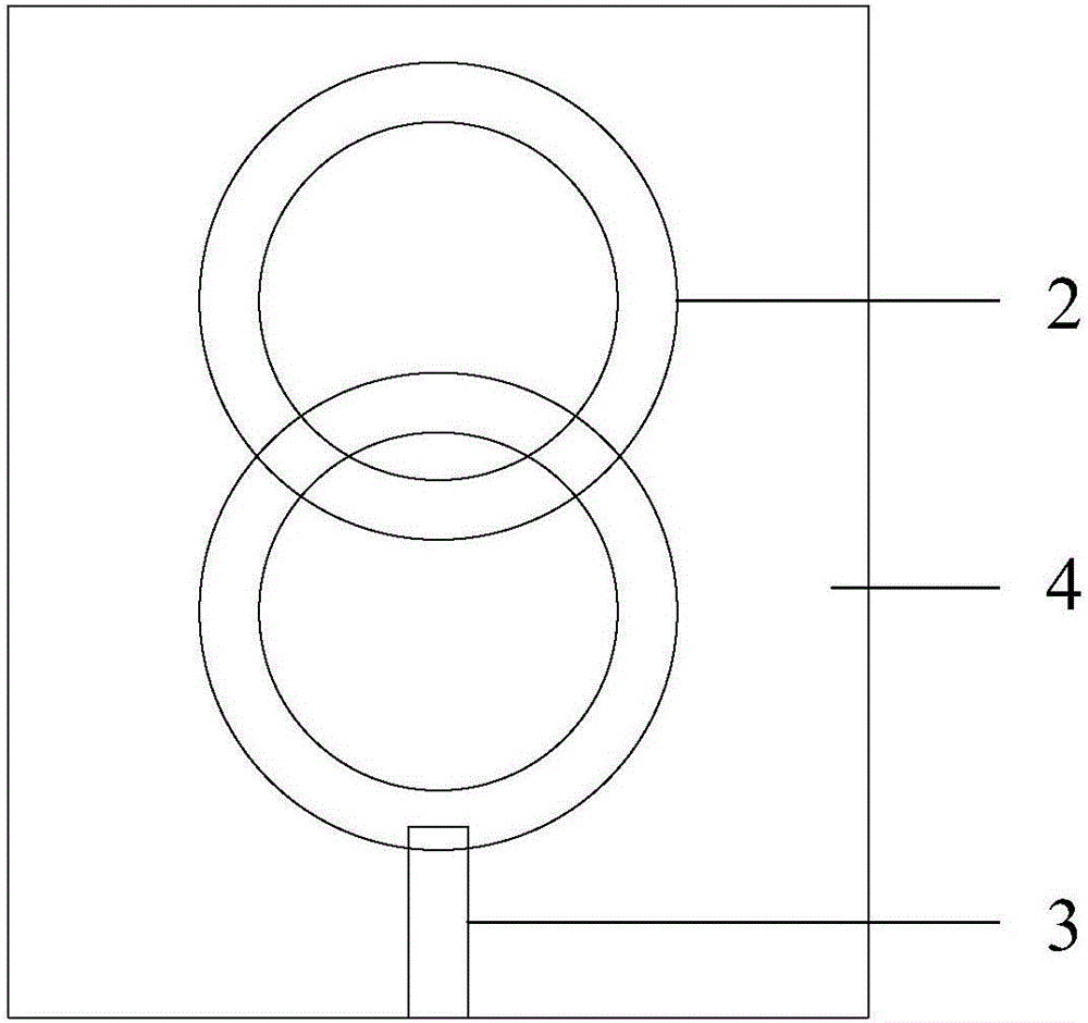
[0027] Embodiment: Two ring-shaped microstrip lines are connected in series to form the radiator 2 of the present invention and embedded in the PCB board. The width of the ring is 4mm, wherein the radius of the outer circle is 10mm, and the radius of the inner circle is 6mm, and the two circles The distance between the centers of the rings is 8mm. One of the rings is connected to a rectangular connector 3 on the outer side of the other ring. The length of the rectangular connector 3 is 11mm, and the overlap length with the ring is 1mm, and the remaining 10mm is not overlapped with the ring. The rectangular connector 3 is connected to the coaxial connector through the dielectric board in the middle of the PCB, and the connecting claws of the coaxial connector are embedded in the floor and connected to the floor.

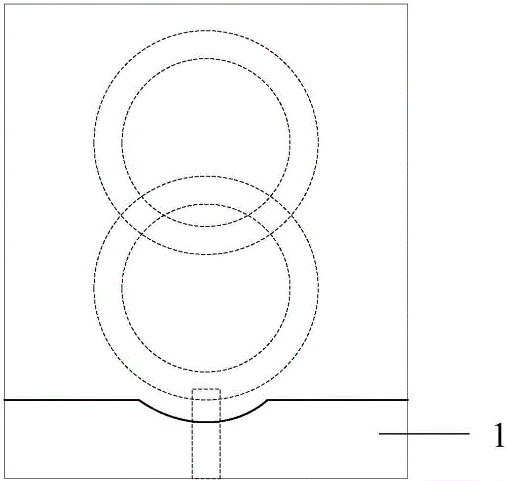
[0028] like figure 2 Shown is the rear view of the PCB board of the present invention.

[0029] The floor is rectangular, embedded in the back of the PCB board, an...


PUM


Abstract

The invention relates to a PCB (Printed Circuit Board) dual-frequency communication antenna. The PCB dual-frequency communication antenna comprises a PCB, a radiating body, a feed-in part and a grounding part, wherein the radiating body and the feed-in part are embedded into the front side of the PCB; the radiating body is connected with the feed-in part, and is used for receiving and transmitting an electromagnetic wave signal; the grounding part is embedded into the back side of the PCB, and is positioned on the same side as the feed-in part. In the PCB dual-frequency communication antenna, a PCB dual-ring series-connection structure is adopted, so that 2.4G and 5.8G are designed integrally, and the antenna is minimized; the working bandwidth of the antenna is extended by an arc-shaped recess between a radiating body projection and a floor, and high gain flatness is achieved; a printed molding antenna technology is adopted, so that the antenna is easy to machine.

Description

technical field [0001] The invention relates to the field of antennas, in particular to a PCB dual-frequency communication antenna. Background technique [0002] PCB (printed) antenna has small working volume, low profile, easy processing, high integration and easy connection with communication equipment, realizing miniaturization of antenna and overall miniaturization of communication equipment, so PCB antenna and communication equipment such as mobile phones and wireless routers Chinese applications have attracted much attention. [0003] The working frequency band of this PCB antenna is 2.4G\5.8G two frequency bands, this frequency includes communication systems such as WiFi, Zigbee, Bluetooth and other ISM applications. [0004] At present, antennas for ISM application communication systems such as Wifi and Zigbee on the market have large working volume, difficult processing, and high cost, and 2.4G and 5.8G are generally designed separately, with low integration. Con...

Claims


Application Information

Patent Timeline
Patent Type & Authority Applications(China)
IPC IPC(8): H01Q1/38H01Q1/48H01Q1/50
CPCH01Q1/38H01Q1/48H01Q1/50
Inventor 杜方孙金段永峰李可陈令山张大伟马芳孙月王蕊张启园刘江红
Owner ALLWIN TELECOMM
Why Eureka
Try Eureka