
Membrane key switch for mining instrument and method for making its shielding layer

A manufacturing method and shielding layer technology, applied in the direction of electric switches, printed circuit manufacturing, conductive pattern formation, etc., can solve problems such as susceptibility to radio frequency and static electricity interference, difficult anti-electromagnetic shielding interference measures, key misoperations, etc., to reduce Electromagnetic interference, guaranteed electromagnetic shielding effect, high electromagnetic shielding efficiency effect

Active Publication Date: 2020-03-06
CHANGZHOU PULIMAI PRECISION ELECTRONICS DEVICE
View PDF6 Cites 0 Cited by
  • Summary
  • Abstract
  • Description
  • Claims
  • Application Information

AI Technical Summary

Problems solved by technology

When the traditional membrane key switch is used as the operation panel, due to two major defects of the membrane key switch, one of them has a large amount of gaps, which brings great difficulties to the shielding of electronic products, and the second is the circuit and components of the switch part. Susceptible to interference from radio frequency and static electricity, resulting in misoperation of button operation
In addition, if this type of membrane switch is to be used in mines, anti-electromagnetic shielding measures are a difficult problem

Method used


Image

  • Membrane key switch for mining instrument and method for making its shielding layer
  • Membrane key switch for mining instrument and method for making its shielding layer
  • Membrane key switch for mining instrument and method for making its shielding layer

Examples


Embodiment 1

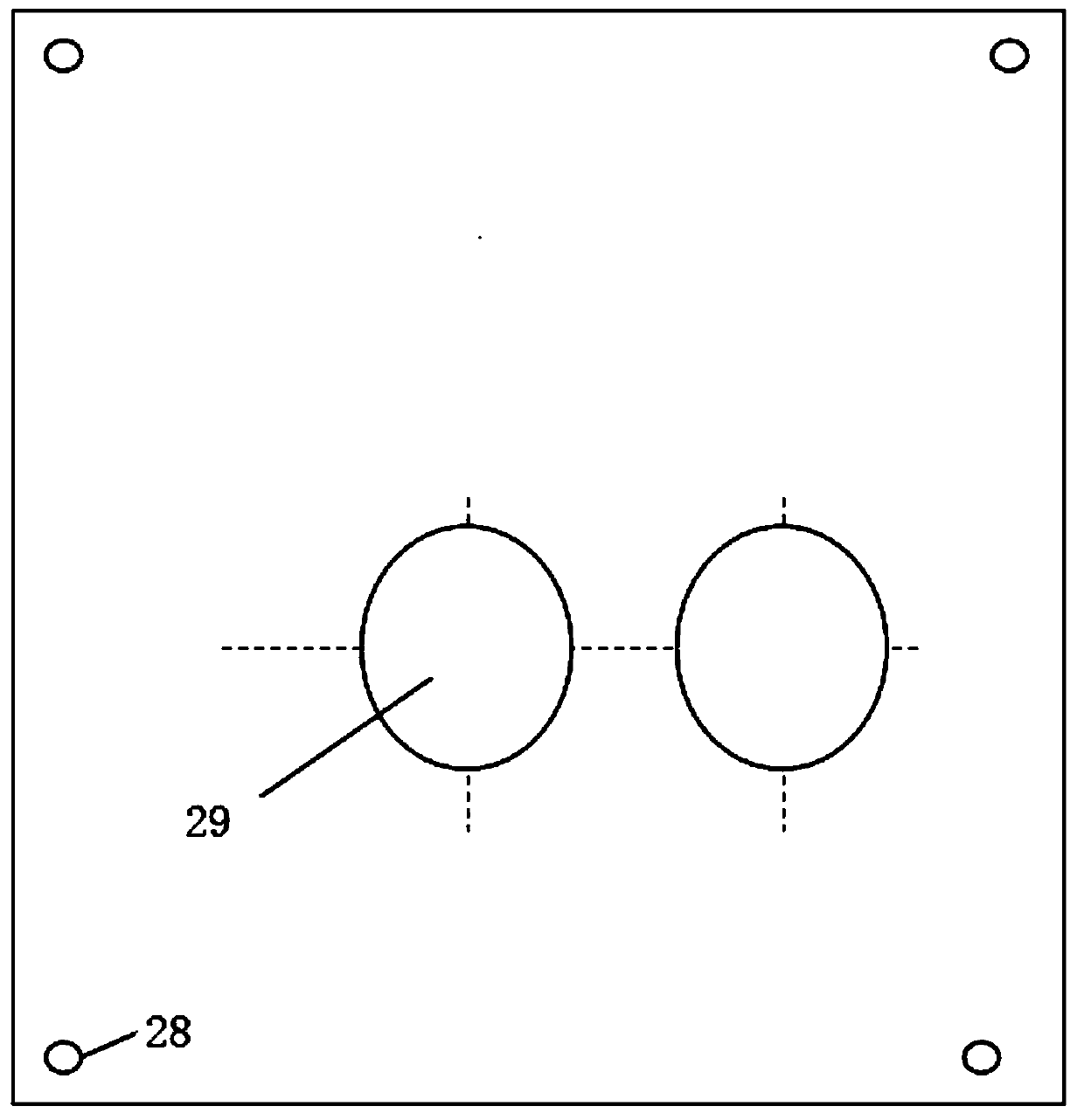
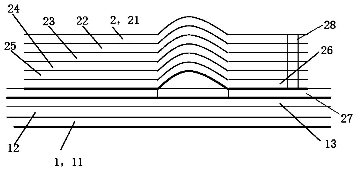
[0035] See figure 1 and figure 2 , a mine meter membrane key switch of this embodiment is composed of a printed circuit board 1 and a membrane key panel 2 covered on the printed circuit board 1; the printed circuit board 1 is followed by a ground layer 11 and a power layer 12 and several signal layers 13; the thin film key panel 2 from top to bottom are: first protective layer 21, PET substrate 22, pattern layer 23, shielding layer 24, second protective layer 25, conductive adhesive layer 26 and key pad Layer 27; PET substrate 22, pattern layer 23, shielding layer 24, second protective layer 25 and conductive adhesive layer 26 are provided with at least one process via 28, shielding layer 24 and conductive adhesive layer 26 are connected; printed circuit board 1 The ground layer 11 is connected to the shielding layer 24 of the membrane key panel 2 . The first protective layer 21 and the second protective layer 25 are UV ink; the shielding layer 24 is conductive paste. The ...


PUM

PropertyMeasurementUnit
Shore hardnessaaaaaaaaaa

Abstract

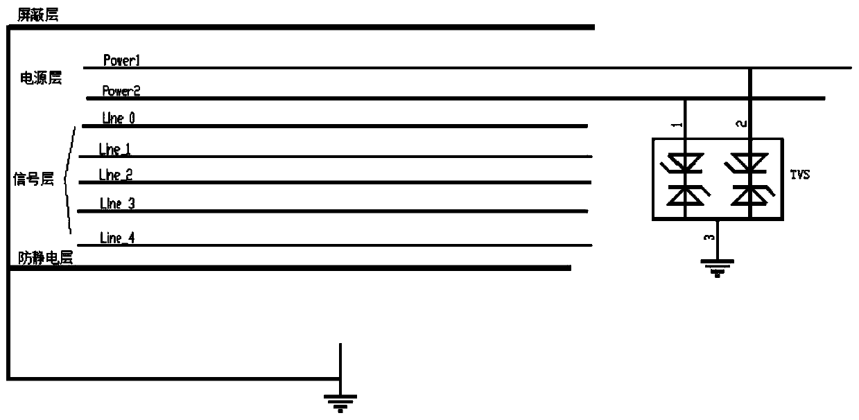
The invention discloses a mining instrument thin-film button switch and a shielding layer making method thereof. The thin-film button switch is composed of a printed circuit board and a thin-film button panel covering the printed circuit board. The printed circuit board is composed of a ground wire layer, a power layer and a plurality of signal layers in sequence from bottom to top. A TVS power protector is connected between the ground wire layer and the power layer. The thin-film button panel is composed of a first protective layer, a PET substrate, a pattern layer, a shielding layer, a second protective layer, a conductive adhesive layer and a button pad layer in sequence from top to bottom. The ground wire layer of the printed circuit board is connected with the shielding layer of the thin-film button panel. The TVS power protector is connected in parallel between the power layer and the ground wire layer to reduce instantaneous electromagnetic interference and protect the thin-film button switch.

Description

technical field [0001] The invention relates to a membrane key switch for a mining instrument and a method for manufacturing the shielding layer thereof. Background technique [0002] As intelligent electronic products continue to be used in coal mines, the types of electronic products that use membrane key switches as operation panels are also increasing. When the traditional membrane key switch is used as the operation panel, due to two major defects of the membrane key switch, one of them has a large amount of gaps, which brings great difficulties to the shielding of electronic products, and the second is the circuit and components of the switch part. It is easy to be interfered by radio frequency and static electricity, which may lead to misoperation of button operation. In addition, if this type of membrane switch is to be used in mines, anti-electromagnetic shielding interference measures are a difficult problem. [0003] For mining electrical products, its explosion...

Claims


Application Information

Patent Timeline
Patent Type & Authority Patents(China)
IPC IPC(8): H01H13/702H01H13/86H05K1/02H05K3/12
CPCH01H13/702H01H13/86H05K1/0224H05K3/1216H05K2201/0715
Inventor 黄宇航杨全会李亮亮
Owner CHANGZHOU PULIMAI PRECISION ELECTRONICS DEVICE
Learn More