
Double-station separating die for high-density pin integrated circuit and using method thereof

An integrated circuit and double-station technology, which is applied in the manufacture of circuits, electrical components, semiconductors/solid-state devices, etc., can solve problems such as pin circuit failure and pin deformation, and achieve the effect of avoiding insufficient strength and meeting strength requirements

Inactive Publication Date: 2017-06-20
TONGLING SANJIA YAMADA TECH
View PDF4 Cites 0 Cited by
  • Summary
  • Abstract
  • Description
  • Claims
  • Application Information

AI Technical Summary

Problems solved by technology

[0004] The technical problem to be solved by the present invention is that when the existing high-density pin integrated circuits are separated, the pins will be deformed, and in severe cases, even the contact between the pins will cause the circuit to fail. Double-station separation mold for electric circuit and its application method

Method used

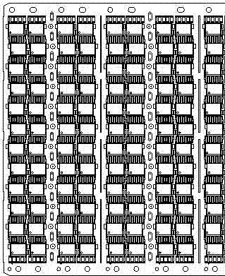

Image

  • Double-station separating die for high-density pin integrated circuit and using method thereof
  • Double-station separating die for high-density pin integrated circuit and using method thereof
  • Double-station separating die for high-density pin integrated circuit and using method thereof

Examples


Embodiment Construction

[0015] The present invention will be further described below in conjunction with the accompanying drawings.

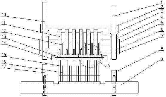
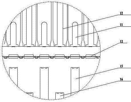
[0016] Such as figure 2 , image 3 As shown, the dual-station separation mold for high-density pin integrated circuits includes an upper die assembly and a lower punch assembly, and the lower punch assembly includes a lower punch base 9 and affixed respectively The first separation station limit column 17 and the second separation station limit column 8 at both ends of the lower punch base, the first separation station limit column is higher than the second separation station limit column, the In the middle of the lower punch base, a first separation punch 15 and a second separation punch 16 are alternately distributed along the horizontal direction, and the height of the first separation punch is higher than the second separation punch; The part includes the upper die base 7 and the first vertical guide rod 10 and the second vertical guide rod 1 passing through the...


PUM


Abstract

The invention discloses a double-station separating die for high-density pin integrated circuit and a using method thereof. The die includes an upper recessed die assembly and a lower protruding die assembly, the lower protruding die assembly includes a lower protruding die base (9) and a first separating station limiting column (17) and a second separating station limiting column (8) fixedly connected with the two ends of the lower protruding die base, the first separating station limiting column is higher than the second separating station limiting column, the middle of the lower protruding die base is alternatively provided with a first separating protruding die (15) and a second separating protruding die (16) at an interval along the horizontal direction, and the first separating protruding die is higher than the second separating protruding die. For the integrated circuit product pin crossing condition, the problem of mutual interference during the product discharging due to the pin crossing can be solved, meanwhile, by means of the double-station separation, the problem that the knife-edge member strength is no enough when the product is separated simultaneously can be effectively prevented, and the strength requirement of the corresponding knife-edge member can be met.

Description

technical field [0001] The invention relates to a separation mold for SOP / TSSOP / SSOP mounting products, in particular to a separation mold for an integrated circuit with high-density cross-pins and a use method thereof. Background technique [0002] With the rapid development of the semiconductor industry, the production process of the basic electronic components of the semiconductor industry has also undergone great changes. In order to meet the requirements of large quantities, high efficiency and low cost, packaging and testing in integrated circuit production is increasingly pursuing high-density product production, which requires packaging as many integrated circuit products as possible within a unit area. Under the existing process conditions, due to the limitation of the processing range of the wire bonding machine, the width of the lead frame is limited within 100mm. Considering the factors of engineering yield and cost, the width of the frame is generally limited in...

Claims


Application Information

Patent Timeline
Patent Type & Authority Applications(China)
IPC IPC(8): H01L21/67H01L21/77
CPCH01L21/67011H01L21/77
Inventor 付小青丁宁李庆生贡喜刘文涛刘正龙
Owner TONGLING SANJIA YAMADA TECH
Learn More