Packaging structure, manufacturing method thereof, and display device

A technology of packaging structure and microstructure, which is applied in semiconductor/solid-state device manufacturing, coating, electrical components, etc., can solve problems such as poor packaging effect of packaging structure, and achieve the effect of improving packaging effect.

Inactive Publication Date: 2017-06-23
BOE TECH GRP CO LTD
View PDF5 Cites 20 Cited by
  • Summary
  • Abstract
  • Description
  • Claims
  • Application Information

AI Technical Summary

Problems solved by technology

[0005] In order to solve the problem of poor encapsulation effect of the encapsulation structure, the present invention provides an encapsulation structure, a manufacturing method thereof, and a display device

Method used


Image

  • Packaging structure, manufacturing method thereof, and display device
  • Packaging structure, manufacturing method thereof, and display device
  • Packaging structure, manufacturing method thereof, and display device

Examples


Embodiment Construction

[0048] In order to make the purpose, technical solutions and advantages of the present invention clearer, the present invention will be further described in detail below in conjunction with the accompanying drawings. Obviously, the described embodiments are only some of the embodiments of the present invention, rather than all of them. Based on the embodiments of the present invention, all other embodiments obtained by persons of ordinary skill in the art without making creative efforts belong to the protection scope of the present invention.

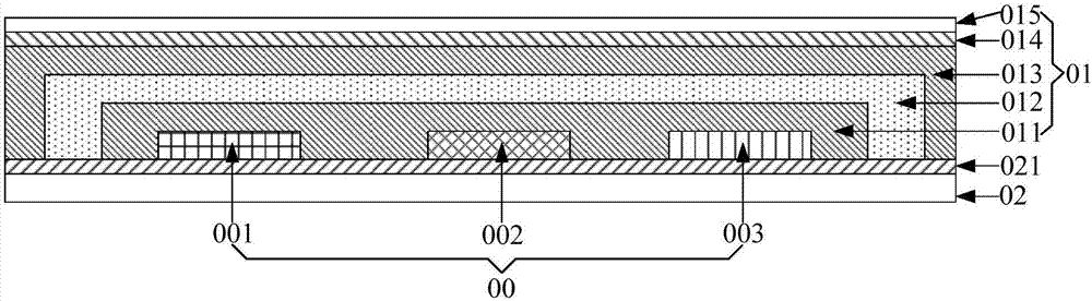
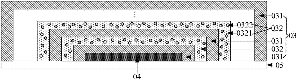
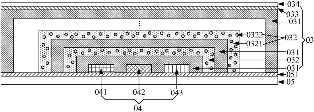
[0049] The OLED device includes an electroluminescence (English: Electro Luminescence; abbreviation: EL) layer, and the EL layer is easily eroded by moisture and oxygen in the air, making the OLED device invalid. Therefore, how to effectively block moisture and oxygen has become a limitation for OLED devices. The main bottleneck of the application. At present, OLED devices are packaged with highly water-resistant hard substrates (such a...


PUM


Abstract

The present invention discloses a packaging structure, a manufacturing method thereof and a display device, and belongs to the packaging field of display devices. The packaging structure includes a plurality of film layers coated on the outer side of a to-be-packaged device. The plurality of film layers are composed of inorganic layers and organic layers, wherein the inorganic layers and the organic layers are stacked up. Each organic layer is composed of a polymer matrix and a repair micro-structure. According to the invention, the problem in the prior art that the packaging effect of a packaging structure is relatively poor can be solved. The packaging structure, the manufacturing method thereof, and the display device are applied to the device packaging field.

Description

technical field [0001] The invention relates to the field of display device packaging, in particular to a packaging structure, a manufacturing method thereof, and a display device. Background technique [0002] Organic Light-Emitting Diode (English: Organic Light-Emitting Diode; abbreviation: OLED) device has the advantages of self-illumination, high brightness, high contrast, low operating voltage, flexible display, etc., and is known as the most promising display device. However, moisture, oxygen and other components in the air have a great influence on the service life of the OLED device. Therefore, it is usually necessary to use an encapsulation structure to encapsulate the OLED device to isolate the OLED device from the air, thereby prolonging the service life of the OLED device. [0003] In related technologies, the encapsulation structure includes an inorganic layer, an organic layer and an inorganic layer that are sequentially stacked and coated on the outside of the...

Claims


Application Information

Patent Timeline
Patent Type & Authority Applications(China)
IPC IPC(8): H01L51/52H01L51/56H01L27/32
CPCH10K59/12H10K50/84H10K71/00C09D133/08C09D133/26C09D133/10H10K59/35H10K50/8445H10K2102/311H10K71/861C09D125/04H10K85/141H10K85/151
Inventor 宋平王菲菲王有为蔡鹏杨静
Owner BOE TECH GRP CO LTD
Why Eureka
Try Eureka