Photolithographic alignment method for manufacturing a semiconductor device

A photolithographic alignment and semiconductor technology, which is applied in the direction of semiconductor devices, semiconductor/solid-state device parts, electric solid-state devices, etc., can solve problems such as difficult identification, unclear marks, and complex structures, and achieve improved recognition rates, Meet the requirements, the effect of simple implementation process

Active Publication Date: 2018-08-14
ZHUZHOU CRRC TIMES SEMICON CO LTD
View PDF6 Cites 0 Cited by
  • Summary
  • Abstract
  • Description
  • Claims
  • Application Information

AI Technical Summary

Problems solved by technology

[0007] In view of this, the purpose of the present invention is to provide a semiconductor device manufacturing lithography alignment method, to solve the existing semiconductor device manufacturing process due to the complexity of the structure of the semiconductor device so that many layers become unclear and difficult to identify when the mark is exposed question

Method used


Image

  • Photolithographic alignment method for manufacturing a semiconductor device
  • Photolithographic alignment method for manufacturing a semiconductor device
  • Photolithographic alignment method for manufacturing a semiconductor device

Examples


Embodiment 1

[0074] as attached Figure 7 To attach Figure 11 As shown, a specific embodiment of a photolithography alignment method for manufacturing a semiconductor device. When the marking area is located in the exposure area, and the marking substance 5 is a liquid substance, the photolithography alignment method includes the following steps:

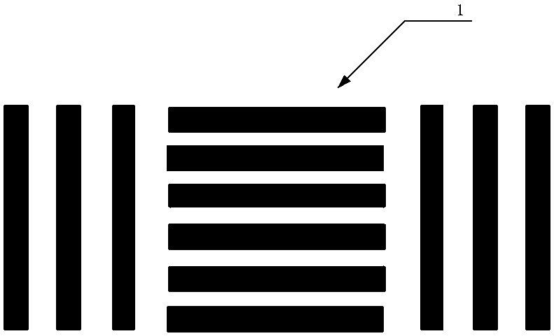
[0075] S1001: After forming an oxide layer on the upper part of the base layer 2, form a photolithographic alignment mark 1 by thin film photolithography or etching, as shown in the attached figure 2 shown;

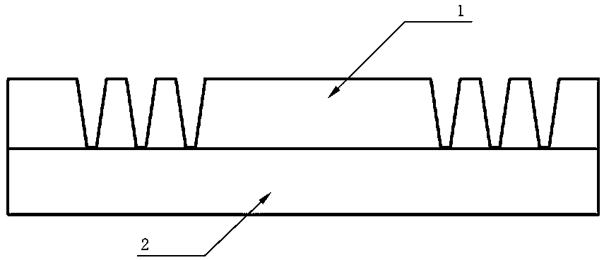
[0076] S1002: grow a metal layer (process alignment layer 3) through the thin film, as attached image 3 shown;

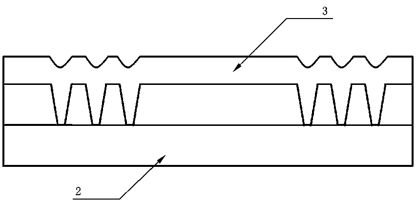
[0077] S101: dripping or depositing a marking substance 5 in the marking area of ​​the process alignment layer 3, as attached Figure 7 As shown; the marking substance 5 uses a negative photoresist to add pigments, so that there is a contrast between the marking substance 5 and the process alignment layer 3, and the exposu...

Embodiment 2

[0085] When the marking area is located in the non-exposed area, and the marking substance 5 is a liquid substance, the photolithographic alignment method includes the following steps:

[0086] S1001: After forming an oxide layer on the upper part of the base layer 2, form a photolithographic alignment mark 1 by thin film photolithography or etching, as shown in the attached figure 2 shown;

[0087] S1002: grow a metal layer (process alignment layer 3) through the thin film, as attached image 3 shown;

[0088] S101: dripping or depositing a marking substance 5 in the marking area of ​​the process alignment layer 3, as attached Figure 7 As shown; the marking substance 5 uses a negative photoresist to add pigments, so that there is a contrast between the marking substance 5 and the process alignment layer 3, and the exposure wavelength of the negative photoresist is different from the exposure wavelength of the positive photoresist;

[0089] S102: remove part of the markin...

Embodiment 3

[0096] When the marking area is located in the exposure area, and the marking substance 5 is a solid substance, the photolithographic alignment method includes the following steps:

[0097] S1001: After forming an oxide layer on the upper part of the base layer 2, form a photolithographic alignment mark 1 by thin film photolithography or etching, as shown in the attached figure 2 shown;

[0098] S1002: grow a metal layer (process alignment layer 3) through the thin film, as attached image 3 shown;

[0099] S101: dripping or depositing a marking substance 5 in the marking area of ​​the process alignment layer 3, as attached Figure 7 Shown; Marking substance 5 adopts POLY (polysilicon) or SIPOS (semi-insulating polysilicon);

[0100] S102: remove part of the marking substance 5, so that only the concave area of ​​the marking area has the marking substance 5, so as to form the secondary alignment mark 4, as attached Figure 8 shown;

[0101] S103: On the basis of the fore...


PUM


Abstract

The invention discloses a photoetching alignment method used in a manufacturing process of a semiconductor device. When a process alignment layer or a photoetching alignment mark is not clear while a base layer has a photoetching alignment mark with a concave-convex type step structure, the process alignment layer is subjected to photoetching alignment; the photoetching alignment method used in manufacturing of the semiconductor device comprises a step of forming secondary alignment marks on the process alignment layer after the process alignment layer is formed on the base layer and before the process alignment layer is subjected to photoresist uniformization. By adoption of the photoetching alignment method, the technical problem of difficulty in identifying unclear marks in exposure of many layers caused by complex structure of the semiconductor device in the manufacturing process of the existing semiconductor device can be solved; mark signals with steps and hard to identify can be optimized; and in addition, the execution steps are simple and easy to implement.

Description

technical field [0001] The invention relates to the field of manufacturing semiconductor devices, in particular to a photolithography alignment method applied to semiconductor devices. Background technique [0002] In the current IC (integrated circuit) production process, a complete chip usually needs to go through more than dozens of photolithography processes. In so many photolithography processes, except for the first photolithography, the remaining levels of photolithography Before exposure, the graphics of this layer must be aligned with the graphics left by the previous layer. However, due to the complex manufacturing process of the semiconductor device structure and the excessive number of photolithography processes, the alignment marks of many layers become unclear and difficult to identify during exposure. Due to the complexity of the semiconductor device structure and process, as well as the complexity of the structure layer and the base layer, the appearance of ...

Claims


Application Information

Patent Timeline
Patent Type & Authority Patents(China)
IPC IPC(8): G03F9/00H01L23/544
Inventor 岳金亮陈辉宋里千程银华刘鹏飞郭可
Owner ZHUZHOU CRRC TIMES SEMICON CO LTD
Why Eureka
Try Eureka