OLED display substrate, manufacturing method of OLED display substrate, display apparatus and encapsulating method of display apparatus

A technology for displaying substrates and manufacturing methods, applied in the fields of final product manufacturing, sustainable manufacturing/processing, semiconductor/solid-state device manufacturing, etc., capable of solving problems such as stress unevenness, poor display of display devices, etc.

Active Publication Date: 2017-07-04
BOE TECH GRP CO LTD
View PDF4 Cites 9 Cited by
  • Summary
  • Abstract
  • Description
  • Claims
  • Application Information

AI Technical Summary

Problems solved by technology

[0003] The OLED display device includes a plurality of light-emitting elements, and each layer of the light-emitting element is solid. Dur

Method used


Image

  • OLED display substrate, manufacturing method of OLED display substrate, display apparatus and encapsulating method of display apparatus
  • OLED display substrate, manufacturing method of OLED display substrate, display apparatus and encapsulating method of display apparatus
  • OLED display substrate, manufacturing method of OLED display substrate, display apparatus and encapsulating method of display apparatus

Examples


Embodiment Construction

[0060] Specific embodiments of the present invention will be described in detail below in conjunction with the accompanying drawings. It should be understood that the specific embodiments described here are only used to illustrate and explain the present invention, and are not intended to limit the present invention.

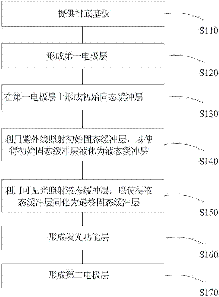
[0061] As an aspect of the present invention, a method for manufacturing an OLED display substrate is provided, wherein, as figure 1 As shown, the manufacturing method includes:

[0062] In step S110, a base substrate is provided;

[0063] In step S120, forming a first electrode layer;

[0064] In step S130, an initial solid buffer layer is formed on the first electrode layer, the material of the initial solid buffer layer includes a component having an azophenyl group in the molecular formula, and the HOMO energy level of the initial solid buffer layer is at Between -6eV and -4.5eV, the LUMO energy level of the initial solid buffer layer is between -3eV and -2...


PUM

PropertyMeasurementUnit
Wavelengthaaaaaaaaaa

Abstract

The invention provides a manufacturing method of an OLED display substrate. The method comprises the following steps: providing an underlayer substrate; forming a first electrode layer; forming an initial solid buffer layer on the first electrode layer, wherein a molecular formula of a material of the initial solid buffer layer has an azobenzene group, a HOMO energy level of the initial solid buffer layer is between -6eV and 4.5eV, and a LUMO energy level of the initial solid buffer layer is between -3eV and 2eV; illuminating the initial solid buffer layer by utilizing ultraviolet, so that the initial solid buffer layer is liquefied to a liquid buffer layer; illuminating the liquid buffer layer by utilizing visible light, so that the liquid buffer layer is solidified into a final solid buffer layer; and forming a luminescent functional layer by virtue of the final solid buffer layer. The invention also provides an OLED display substrate, an encapsulation method of a display apparatus and a display apparatus. The display apparatus is relatively high in yield.

Description

technical field [0001] The present invention relates to the field of display technology, in particular, to a method for manufacturing an OLED display substrate, an OLED display substrate, a packaging method for a display device, a display device obtained by using the packaging method, and a display device comprising the OLED display substrate for display devices. Background technique [0002] OLED display devices have the advantages of fast response speed, thinness, etc., and are more and more popular among users. [0003] The OLED display device includes a plurality of light-emitting elements, and each layer of the light-emitting element is solid. During manufacture, defects such as stress or unevenness are prone to occur. Therefore, the display device may have poor display due to this. [0004] Therefore, how to reduce the display defects of OLED display devices has become a technical problem to be solved urgently in this field. Contents of the invention [0005] The o...

Claims


Application Information

Patent Timeline
IPC IPC(8): H01L51/56H01L51/52
CPCH10K50/8426H10K50/844H10K71/00Y02E10/549Y02P70/50H10K77/111H10K50/15H10K50/17H10K50/81H10K2101/30H10K30/865H10K50/841H10K85/141
Inventor 高昕伟
Owner BOE TECH GRP CO LTD
Why Eureka
Try Eureka