Dual-sided substrate integrated circuit package including a leadframe having leads with increased thickness

a dual-sided substrate and integrated circuit technology, applied in the direction of electrical equipment, semiconductor devices, semiconductor/solid-state device details, etc., can solve the problems of leadframe not being able to bridge the gap between contacts on the circuit board without some modification of the leadframe, laminate structure requires costly, complex manufacturing processes, and is less prone to defects. , the effect of less cost and easy manufacturing

Active Publication Date: 2005-08-18
DELPHI TECH IP LTD
View PDF6 Cites 4 Cited by
  • Summary
  • Abstract
  • Description
  • Claims
  • Application Information

AI Technical Summary

Benefits of technology

[0014] An advantage of the present invention is that the leadframes are less prone to defects, less expensive, and easier to manufacture than leadframes having doubled over lead tips or laminate structures. The undulated leadframes of the present invention have substantially less stress on the base copper and plating material than do doubled over leadframes, so there is considerably less risk of stress fractures across the formed edges. The offset formed or corrugated formed leads of the present invention provide more stress relief inside the integrated circuit package than do flat or doubled over leads.
[0015] Another advantage is that the stock width of the coiled or strip copper material used to make the leadframes can be narrower and less expensive than that used to make leadframes having doubled over lead tips. Thus, the present invention provides a reduction of scrap copper material blanked from the progressive die
[0016] Yet another advantage is that the progressive die can be smaller, more inexpensive to build, and less complicated by virtue of having fewer components and because all of the leads can be formed in one stage. The smaller progressive die can be run in a smaller press with less tonnage, which is more economical to operate.
[0017] A further advantage is that there is no need for a secondary die or bending fixture. Less force is required to undulate the leadframe member because the thickness of the leadframe material is not substantially compressed.
[0018] A still further advantage is that the effective thickness of the leadframe member tips can be controlled by the form punches in the progressive die for the leadframe. This allows the thickness of the copper leadframe material to be less than the thickness of the integrated circuit silicon die. Therefore, a standard thickness of copper material can be selected for the leadframe to be used with a variety of silicon die of different thicknesses. This eliminates the need to special order a custom thickness leadframe to match a specific integrated circuit die thickness per each electronic package application using flat leadframes without doubled over member tips.

Problems solved by technology

This can create design and manufacturing challenges when it becomes necessary to place such miniature components in communication with these larger circuits, assemblies or components.
Since the thickness of the die is generally greater than that of the leadframe, the leadframe may not be able to bridge the gap between contacts on the circuit boards without some modification to the leadframe.
The leadframe can be provided with a laminate structure to increase its thickness, but a laminate structure requires costly, complex, and time consuming manufacturing processes.
In addition, a laminate structure can negatively impact the flexibility of the leadframne and therefore may not be suitable for some assemblies.
A problem with the technique of doubling over the leadframe member tip is that it requires either a large progressive die with multiple stages to flatten the leadframe member tip, or an additional secondary die or bending fixture.
This tight form on the leads work hardens the base copper and plating material, and can create stress cracks across the hem where the leadframe member tip is doubled over.

Method used


Image

  • Dual-sided substrate integrated circuit package including a leadframe having leads with increased thickness
  • Dual-sided substrate integrated circuit package including a leadframe having leads with increased thickness
  • Dual-sided substrate integrated circuit package including a leadframe having leads with increased thickness

Examples


Embodiment Construction

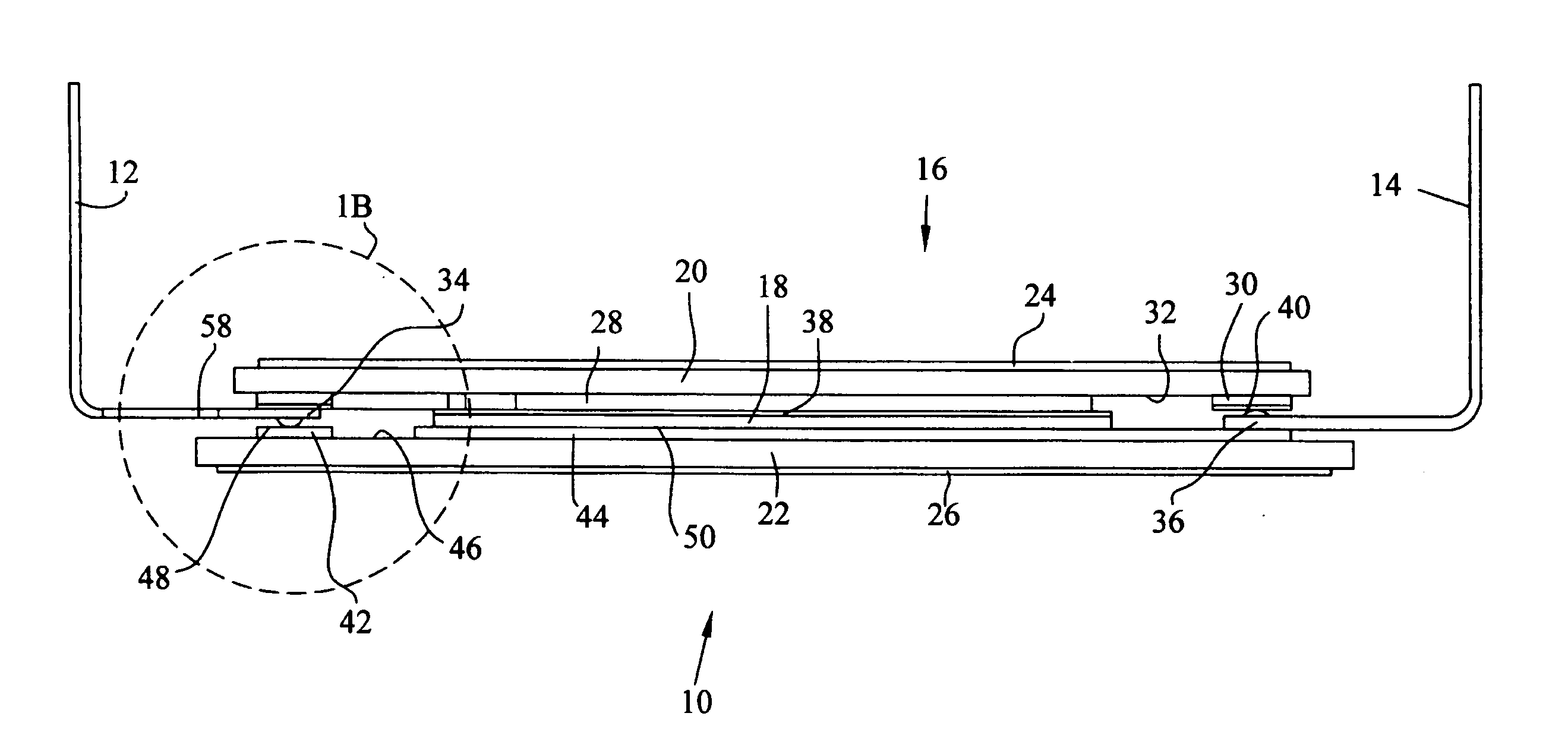
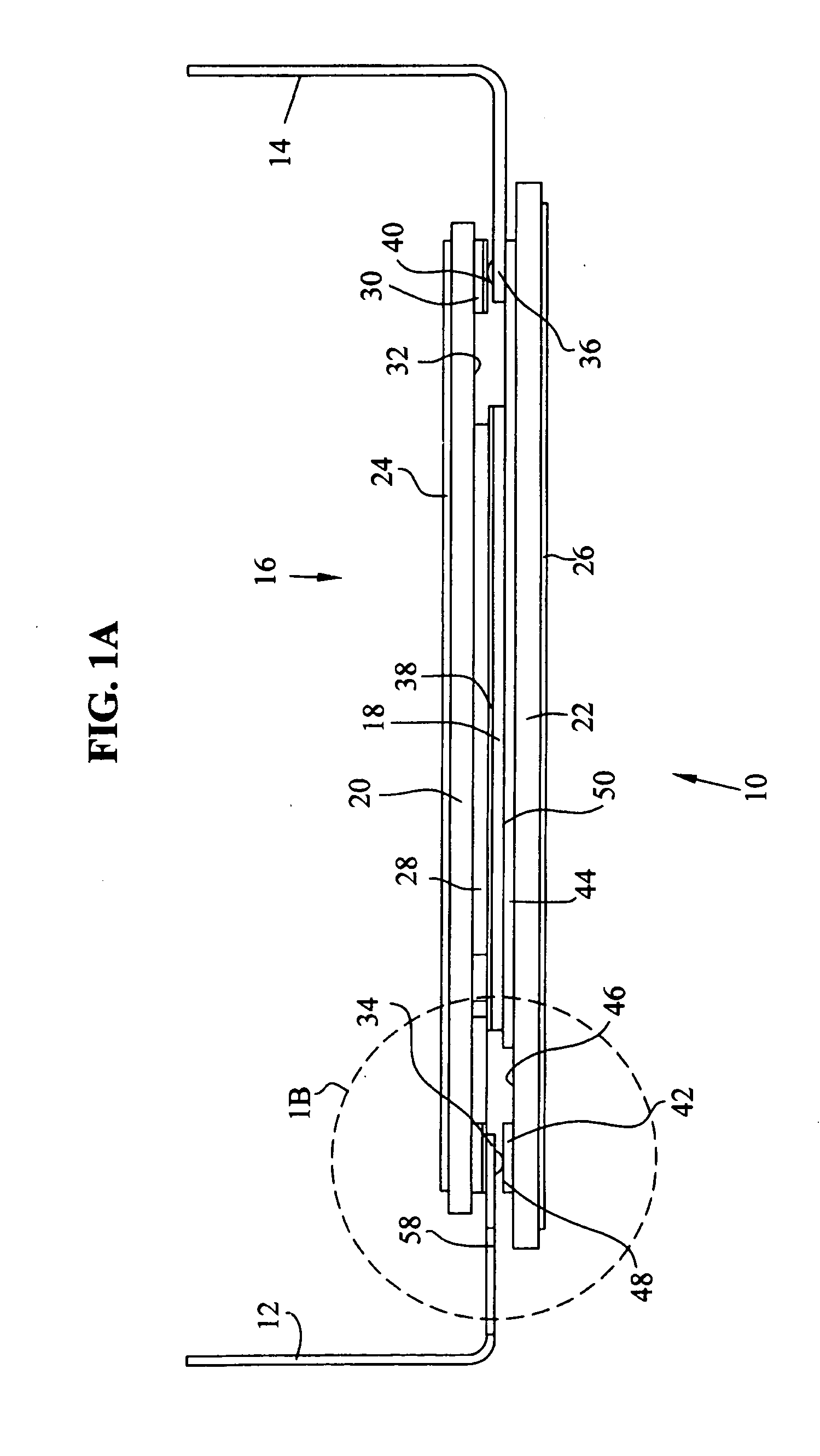
[0056] Referring now to the drawings, and particularly to FIG. 1A, there is shown one embodiment of an integrated circuit package 10 of the present invention, including leadframes 12, 14 in electrical communication with an integrated circuit 16. Integrated circuit 16 includes an integrated circuit die 18 formed of a semiconductor material. Die 18 is sandwiched between non-conductive substrates 20, 22, which can be formed of a ceramic material.

[0057] Each of substrates 20, 22 can include a respective layer of solderable material 24, 26 on the outer surfaces thereof. Pressure attached applications may not require solderable material 24, 26 on the outer surface. Elimination of solderable material 24 and 26 reduces the thermal resistance and device temperature.

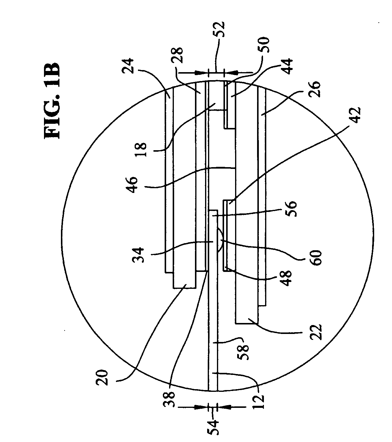
[0058] Electrically conductive bonded copper elements 28, 30 are attached to an inner surface 32 of substrate 20. In the particular embodiment shown in FIG. 1A, element 28 is in the form of a substrate, while element 30 may bett...


PUM

PropertyMeasurementUnit
angleaaaaaaaaaa
thicknessaaaaaaaaaa
conductiveaaaaaaaaaa

Abstract

An integrated circuit package includes a first non-conductive substrate having a first inner surface and a second non-conductive substrate having a second inner surface. A die having a first thickness is disposed between the first and second inner surfaces. A leadframe includes a member having a proximal end and a distal end. The proximal end has a second thickness less than the first thickness. The distal end is disposed between the first and second inner surfaces. The distal end is undulated such that the distal end has an effective thickness greater than the second thickness.

Description

TECHNICAL BACKGROUND [0001] This invention relates generally to a dual-sided substrate integrated circuit package, and, more particularly, to a leadframe included in a dual-sided substrate integrated circuit package. BACKGROUND OF THE INVENTION [0002] Miniaturized electronic components, such as chip transistors, processors, etc., must often be assembled in conjunction with circuits, assemblies or components of comparatively larger dimensions. This can create design and manufacturing challenges when it becomes necessary to place such miniature components in communication with these larger circuits, assemblies or components. [0003] One solution to such manufacturing problems has been through the use of leadframes. A leadframe is a thin layer of metal that connects the wiring from tiny electrical terminals on the semiconductor surface to the large-scale circuitry on electrical devices and circuit boards. Leadframes provide an electrical conduit from the multiple small terminals commonl...

Claims


Application Information

Patent Timeline
Patent Type & Authority Applications(United States)
IPC IPC(8): H01L21/44H01L23/495H01L23/498
CPCH01L23/49833H01L23/49861H01L2924/0002Y10T29/49121Y10T29/49222H01L2924/00
Inventor MOCK, ROGER A.GERBSCH, ERICH W.
Owner DELPHI TECH IP LTD
Why Eureka
Try Eureka