Optical lens group for imaging, imaging device and electronic device

An optical lens, lens technology, applied in optics, optical components, instruments, etc., can solve problems such as insufficient imaging range and poor resolution

Active Publication Date: 2019-08-27
LARGAN PRECISION
View PDF4 Cites 0 Cited by
  • Summary
  • Abstract
  • Description
  • Claims
  • Application Information

AI Technical Summary

Problems solved by technology

It is known that the optical systems currently on the market are often difficult to achieve both a large viewing angle and a large aperture at the same time, which is likely to cause problems such as insufficient imaging range or poor resolution under low light sources.

Method used


Image

  • Optical lens group for imaging, imaging device and electronic device
  • Optical lens group for imaging, imaging device and electronic device
  • Optical lens group for imaging, imaging device and electronic device

Examples


no. 1 example

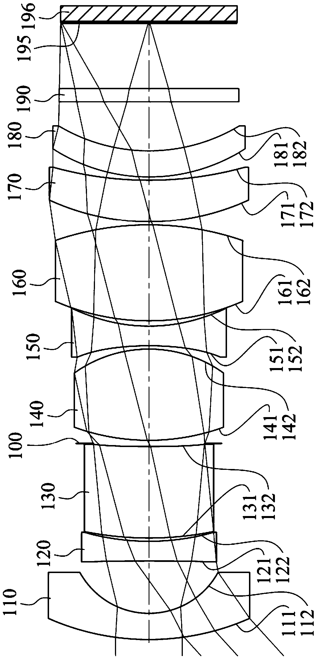
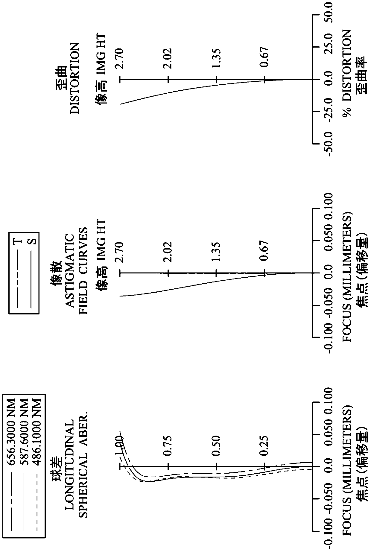
[0121] Please refer to figure 1 and figure 2 ,in figure 1 A schematic diagram showing an imaging device according to the first embodiment of the present invention, figure 2 From left to right are the spherical aberration, astigmatism and distortion curves of the first embodiment. Depend on figure 1 It can be seen that the image capturing device of the first embodiment includes an image capturing optical lens group (not another number) and an electronic photosensitive element 196 . The optical lens group for taking images includes a front mirror group (not otherwise labeled), an aperture 100, a rear mirror group (not otherwise labeled), an infrared filter element 190, and an imaging surface 195 from the object side to the image side, and the electronic The photosensitive element 196 is disposed on the imaging surface 195 of the image-taking optical lens group, wherein the total number of lenses in the image-taking optical lens group is eight. In detail, the total number ...

no. 2 example

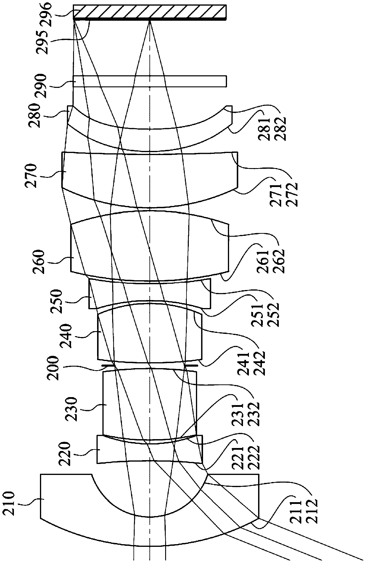
[0156] Please refer to image 3 and Figure 4 ,in image 3 A schematic diagram showing an imaging device according to a second embodiment of the present invention, Figure 4 From left to right are the spherical aberration, astigmatism and distortion curves of the second embodiment. Depend on image 3 It can be seen that the image capturing device of the second embodiment includes an image capturing optical lens group (not another number) and an electronic photosensitive element 296 . The optical lens group for taking images includes a front mirror group (not otherwise labeled), an aperture 200, a rear mirror group (not otherwise labeled), an infrared filter element 290, and an imaging surface 295 from the object side to the image side, and the electronic The photosensitive element 296 is disposed on the imaging surface 295 of the image-taking optical lens group, wherein the total number of lenses in the image-taking optical lens group is eight. Specifically, the total num...

no. 3 example

[0174] Please refer to Figure 5 and Figure 6 ,in Figure 5 A schematic diagram showing an imaging device according to a third embodiment of the present invention, Figure 6 From left to right are the spherical aberration, astigmatism and distortion curves of the third embodiment. Depend on Figure 5 It can be seen that the image capturing device of the third embodiment includes an image capturing optical lens group (not another number) and an electronic photosensitive element 396 . The optical lens group for taking images includes a front mirror group (not otherwise labeled), an aperture 300, a rear mirror group (not otherwise labeled), an infrared filter element 390, and an imaging surface 395 from the object side to the image side, and the electronic The photosensitive element 396 is disposed on the imaging surface 395 of the image-taking optical lens group, wherein the total number of lenses in the image-taking optical lens group is eight. Specifically, the total num...


PUM


Abstract

The invention discloses an optical lens set for image capture, an image capture device, and an electronic device. The optical lens set for image capture comprises a front lens group, a diaphragm and a rear lens group in sequence from the object side to the image side. The front lens group comprises at least two lenses, and the lens closest to a shot object has negative refracting power and has a concave image-side surface. The rear lens group comprises at least four lenses, and the lens closest to the imaging plane has a concave image-side surface. When specific conditions are satisfied, the space of the optical lens set for image capture can be fully utilized, and the complexity and difficulty of assembly can be reduced. The invention further discloses an image capture device with the optical lens set for image capture, and an electronic device with the image capture device.

Description

technical field [0001] The present invention relates to an optical lens group for taking images and an image taking device, and in particular to an optical lens group for taking images with a wide viewing angle and an image taking device applied to electronic devices. Background technique [0002] In recent years, with the gradual popularization of lens types and uses, many products (such as home appliances, game consoles, monitors, automobiles, electronic products and mobile devices, etc.) are equipped with lenses, which are suitable for image assistance, image recognition, Motion detection and other functions. The lens on some devices must have a large viewing angle, and can even operate under light sources or environments with low light levels (such as night surveillance systems or car monitors). It is known that the optical systems currently on the market are often difficult to achieve both a large viewing angle and a large aperture at the same time, which is likely to ...

Claims


Application Information

Patent Timeline
Patent Type & Authority Patents(China)
IPC IPC(8): G02B13/00
Inventor 谢东益黄炫钦陈纬彧
Owner LARGAN PRECISION
Why Eureka
Try Eureka