Bonding structure, flexible screen body with bonding structure and manufacturing method thereof

A flexible screen, flexible technology, applied in semiconductor/solid-state device manufacturing, semiconductor devices, nonlinear optics, etc., can solve the problems of reducing the yield rate of flexible screens, wire breakage, defective products, etc., to improve the peeling yield, avoid The effect of stress concentration and reducing the risk of the line being pulled off

Active Publication Date: 2017-08-01
KUNSHAN NEW FLAT PANEL DISPLAY TECH CENT
View PDF3 Cites 4 Cited by
  • Summary
  • Abstract
  • Description
  • Claims
  • Application Information

AI Technical Summary

Problems solved by technology

Taking bonding as an example, there are usually chips and other components bonded in the bonding area on the flexible screen, and there are often a large number of circuits distributed around the chip, so the peeling operation between the flexible screen and the substrate must be very careful, otherwise it will easily lead to Defective products caused by line damage
[0003] In the prior art, the substrate A is located under the flexible screen, and due to the obvious hardness difference between the chip B in the bonding area and the flexible screen C itself, a large stress will be generated in the bonding area during actual peeling ( like figure 1 As shown), stress concentration is formed at the position of chip B (point D refers to the stress concentration area), which can easily lead to the breakage of the circuit at this position, thereby greatly reducing the yield rate of peeling after flexible screen bonding

Method used


Image

  • Bonding structure, flexible screen body with bonding structure and manufacturing method thereof
  • Bonding structure, flexible screen body with bonding structure and manufacturing method thereof
  • Bonding structure, flexible screen body with bonding structure and manufacturing method thereof

Examples


Embodiment 1

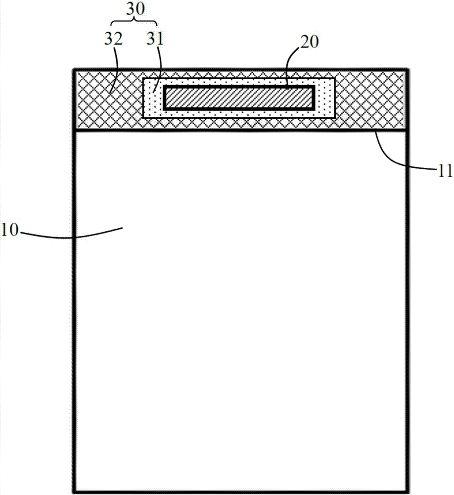
[0029] In order to solve the problem of low peeling yield of the existing flexible screen, the embodiment of the present invention provides a bonding structure for the flexible screen, refer to figure 2 As shown, the flexible screen includes a display area 10 , a bonding area 11 connected to the display area 10 and a chip 20 installed in the bonding area. The bonding area 11 is provided with a flexible protective layer 30 surrounding the chip 20, wherein the flexible protective layer 30 includes a first protective layer 31 arranged around the chip 20, and a first protective layer arranged on the first protective layer The second protective layer 32 on the periphery of 31, the first protective layer 31 and the second protective layer 32 are made of different materials but both are flexible materials, and the thickness of the first protective layer 31 is greater than that of the second protective layer 32 .

[0030] Wherein, the flexible screen is provided with a bonding area 1...

Embodiment 2

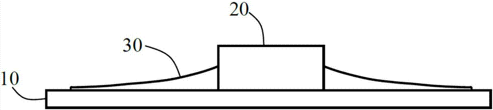
[0033] An embodiment of the present invention provides a flexible screen bonding area structure. An embodiment of the present invention provides a bonding structure for a flexible screen. Refer to figure 2 As shown, the flexible screen includes a display area 10, a bonding area 11 connected to the display area 10, and a chip 20 installed in the bonding area. The bonding area 11 is provided with a flexible protective layer 30 surrounding the chip 20, the flexible protective layer 30 is a single material adhesive layer, which is coated in the bonding area 11 of the flexible screen, and the flexible protective layer The thickness of the layer 30 gradually becomes thicker towards the direction of the chip 20, such as image 3 As shown, that is, the thickness of the flexible protective layer 30 at the edge of the bonding region 11 is smaller than the thickness at the peripheral edge of the chip 20, so that the flexible protective layer 30 with gradually changing thickness can form...

Embodiment 3

[0035] An embodiment of the present invention provides a method for preparing a flexible screen body bonding structure, including the following steps:

[0036] S01: Setting a bonding area on the surface of the flexible screen, and bonding chips in the bonding area; and

[0037] S02: Set up a flexible protective layer around the chip.

[0038] Wherein, in the above S02, "setting a flexible protective layer around the chip" includes: setting a first protective layer around the chip, so that the first protective layer is respectively connected to the surface of the chip and the flexible screen; setting a second protective layer around the first protective layer. layer, and the thickness of the second protective layer is smaller than the thickness of the first protective layer.

[0039] Preferably, the "setting the first protective layer" refers to coating the UV adhesive layer, and irradiating the UV adhesive layer with ultraviolet light to make it cured. The "setting the secon...


PUM


Abstract

The invention discloses a flexible screen bonding area structure and a manufacturing method thereof. The flexible screen bonding area structure is provided with a flexible screen and a chip arranged on the surface of the flexible screen; the flexible screen is provided with a bonding area for bonding the chip; the bonding area is coated with a flexible protection layer; and the flexible protection layer surrounds the chip. In comparison with the prior art, through forming the flexible protection layer with a different hardness around the chip, the stress generated around the chip in the case of debonding can be greatly dispersed, hierarchy stress is formed, stress gathering at the position closely around the chip can be avoided, the risk that a line around the chip is pulled broken can be reduced, and the debonding yield of the flexible screen is finally improved.

Description

technical field [0001] The invention relates to the technical field of display panels, in particular to a flexible screen bonding region structure and a preparation method thereof. Background technique [0002] In the field of flexible display manufacturing, due to its fragile material, the flexible screen is very easy to be damaged during the manufacturing process. Therefore, in practice, it is usually necessary to attach it to a substrate (such as tempered glass), and then perform circuit etching, Bonding and other steps, and finally the flexible screen is separated from the substrate by peeling off. Taking bonding as an example, there are usually chips and other components bonded in the bonding area on the flexible screen, and there are often a large number of circuits distributed around the chip, so the peeling operation between the flexible screen and the substrate must be very careful, otherwise it will easily lead to Defective products caused by line damage. [0003...

Claims


Application Information

Patent Timeline
Patent Type & Authority Applications(China)
IPC IPC(8): H01L27/12H01L21/77
CPCH01L21/77H01L27/12H01L23/3135G02F1/133305G02F1/13454G02F2201/50G02F2202/023G09F9/301
Inventor 张秀玉王宝友党鹏乐丁立薇张小宝朱晖
Owner KUNSHAN NEW FLAT PANEL DISPLAY TECH CENT
Why Eureka
Try Eureka