
Liquid crystal display panel, press fit method thereof, and liquid crystal display

A liquid crystal display panel and display area technology, applied in the direction of instruments, nonlinear optics, optics, etc., can solve problems such as process complexity and cost waste, and achieve the effect of reducing the number of coating times and reducing production costs

Inactive Publication Date: 2017-08-04
WUHAN CHINA STAR OPTOELECTRONICS TECH CO LTD
View PDF3 Cites 3 Cited by
  • Summary
  • Abstract
  • Description
  • Claims
  • Application Information

AI Technical Summary

Problems solved by technology

In the prior art, the assembly of the liquid crystal display panel, the flexible circuit board, the chip module, etc. is fixed with conductive glue, but in the production process, the fixing of the flexible circuit board and the chip module needs to be carried out many times because of the need for different conductive glues. Coating, resulting in complicated process and waste of cost

Method used


Image

  • Liquid crystal display panel, press fit method thereof, and liquid crystal display
  • Liquid crystal display panel, press fit method thereof, and liquid crystal display
  • Liquid crystal display panel, press fit method thereof, and liquid crystal display

Examples


Embodiment Construction

[0024] The following will clearly and completely describe the technical solutions in the embodiments of the present invention with reference to the drawings in the embodiments of the present invention. Wherein, the accompanying drawings are only used for exemplary illustration, and represent only schematic diagrams, and should not be understood as limitations on this patent.

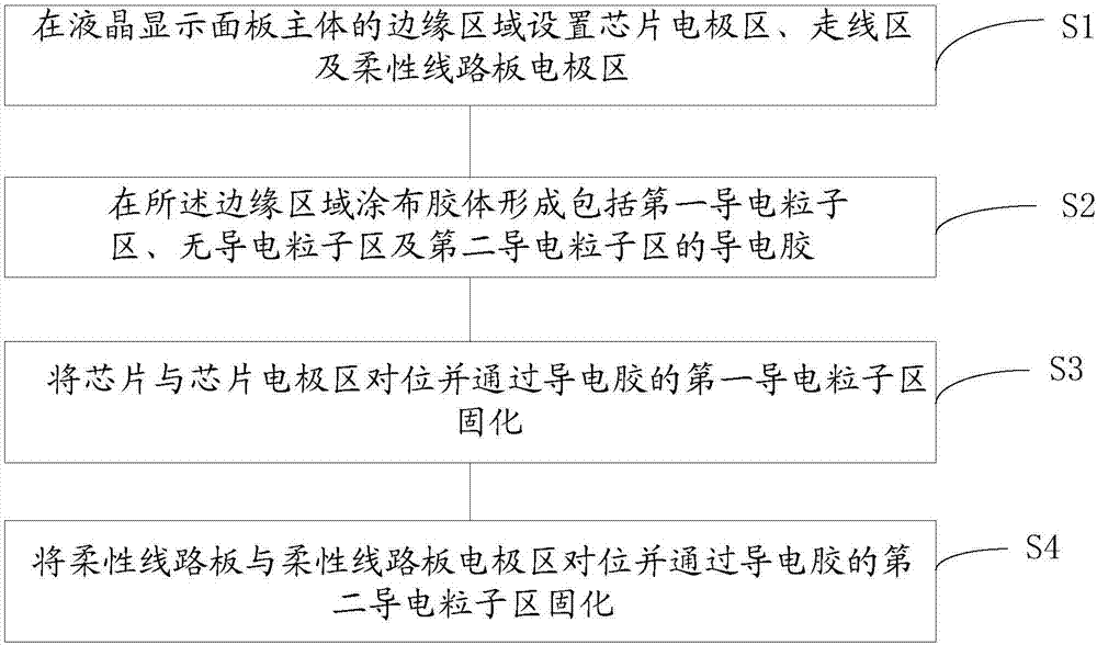
[0025] The present invention provides a liquid crystal display panel and a liquid crystal display (not shown in the figure), wherein a backlight module of the liquid crystal display is attached to the liquid crystal display panel to provide a light source for the liquid crystal display panel. Please also refer to figure 1 and figure 2 , the liquid crystal display panel includes a liquid crystal display panel main body 10 , a flexible circuit board 20 , a chip device 30 and a conductive glue 40 , and the liquid crystal display panel main body 10 includes a display area 11 and an edge area 12 . The edge...


PUM


Abstract

The invention provides a liquid crystal display panel. The liquid crystal panel comprises a liquid crystal panel body, a flexible circuit board and a chip device, the liquid crystal panel body comprises a display area and an edge area, and further comprises a conducting gum, the edge area comprises a chip binding electrode area, a routing area and a flexible circuit board binding electrode area, the chip binding electrode area, the routing area and the flexible circuit board binding electrode area are arranged at intervals, the conducting gum comprises a first conducting particle area, an area free of conducting particles and a second conducting particle area, the particle concentration of the first conducting particle area is larger than that of the second conducting particle area, the conducting gum covers the edge area, the first conducting particle area covers the chip binding electrode area, the area free of the conducting particles covers the routing area, the second conducting particle area covers the flexible circuit board binding electrode area, the flexible circuit board is connected with the flexible circuit board binding electrode area through the second conducting particle area, and the chip device is fixedly connected with the chip binding electrode area through the first conducting particle area.

Description

technical field [0001] The invention relates to the technical field of liquid crystal displays, in particular to a liquid crystal display panel, a pressing method thereof, and a liquid crystal display. Background technique [0002] With the development of display technology, consumers not only have higher and higher requirements for the display effect of liquid crystal display screens, but also have increasingly high requirements for cost. The liquid crystal display panel in the display screen is connected to the backlight module through a flexible circuit board. In the prior art, the assembly of the liquid crystal display panel, the flexible circuit board, the chip module, etc. is fixed with conductive glue, but in the production process, the fixing of the flexible circuit board and the chip module needs to be carried out many times because of the need for different conductive glues. Coating causes the complexity of the process and wastes the cost. Contents of the inventi...

Claims


Application Information

Patent Timeline
Patent Type & Authority Applications(China)
IPC IPC(8): G02F1/1333G02F1/13
CPCG02F1/1333G02F1/1303
Inventor 左清成袁小玲
Owner WUHAN CHINA STAR OPTOELECTRONICS TECH CO LTD
Learn More