Multi-layered PCB and processing method therefor

A processing method and unique technology, applied in the direction of multi-layer circuit manufacturing, circuit board tool positioning, printed circuit components, etc., can solve problems such as low efficiency, consuming a lot of time and manpower, unable to effectively solve problems, etc., to improve product quality Effect

Active Publication Date: 2017-08-11
DONGGUAN WERY DOOD CIRCUIT BOARD EQUIP
View PDF13 Cites 11 Cited by
  • Summary
  • Abstract
  • Description
  • Claims
  • Application Information

AI Technical Summary

Problems solved by technology

In the process of process quality traceability, because the outer layer copper foil and the inner layer are laminated together, and the inner layer is formed by the fusion of multiple core boards, the correlation between the outer layer information and ...

Method used


Image

  • Multi-layered PCB and processing method therefor
  • Multi-layered PCB and processing method therefor

Examples


Embodiment 1

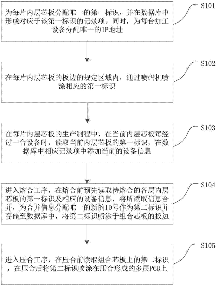
[0040] see figure 1 , a kind of processing method of multilayer PCB is provided in the present embodiment, comprises the following steps:

[0041] Step S101 , assigning a unique first identifier to each inner core board, and forming a record item corresponding to the first identifier in the database. At the same time, assign a unique IP address to each device.

[0042] In this step, a unique ID code can be assigned to each inner core board according to the work order. The ID code is used as the first identification, and its information includes model, batch number, and core board number.

[0043] Step S102 , in the specified area of ​​the board edge of each inner layer core board, spray the corresponding first logo with the inkjet printer.

[0044] Step S103. In the production process of each inner core board, when the current inner core board passes through a piece of equipment, read the first identification of the current inner core board, and add the current ID to the cor...

Embodiment 2

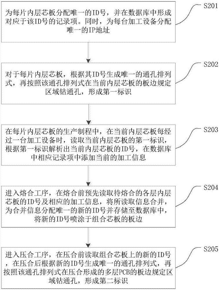
[0055] In the first embodiment, the first mark on the inner core board and the second mark on the multi-layer PCB are formed by spraying with an inkjet printer. However, in the process of production and use, the first mark and the second mark may be adversely affected by being covered due to external factors, making the mark display not clear enough to be easily read. Based on improvements.

[0056] see figure 2 , the processing method of a kind of new multi-layer PCB that present embodiment provides, comprises steps:

[0057]Step S201, assigning a unique ID code to each inner core board, and forming a record item corresponding to the ID code in the database. At the same time, assign a unique IP address to each device.

[0058] Step S202 , for each inner core board, generate a unique through hole arrangement according to its ID code, and then drill through holes in a specified area of ​​the current inner core board according to the through hole arrangement to form a first ...

Embodiment 3

[0072] In this embodiment, a multi-layer PCB is provided, which is made by using Embodiment 1 or Embodiment 2. The outer layer forms identification information formed by spraying or drilling, and the relevant information of each inner layer can be obtained according to the identification information, so as to realize Quality traceability throughout the process.


PUM


Abstract

The invention discloses a multi-layered PCB and a processing method therefor. The processing method comprises the steps of setting a unique first identifier on a current inner layer core board at the initial moment in the manufacturing process of each inner layer core board; reading the first identifier of the current inner layer core board when the current inner layer core board passes through each equipment, and recording the current equipment information in a corresponding position in a database; in a fusing process, pre-reading the first identifier of each to-be-fused inner layer core board in each layer and corresponding equipment information, and synthesizing the read information to generate a unique second identifier, and setting the second identifier on a combined core board which is formed by fusing; and in a laminating process, pre-reading the second identifier on the combined core board, and setting the second identifier on the multi-layered PCB which is formed by lamination. According to the embodiments disclosed in the invention, the outer layer information of the multi-layered PCB is obtained by combination of information of each inner layer, so that a working staff can carry out efficient and accurate quality tracking according to the outer layer identification information.

Description

technical field [0001] The invention relates to the technical field of circuit boards, in particular to a multilayer PCB processing method and the multilayer PCB. Background technique [0002] PCB, also known as printed circuit board, printed circuit board, or printed board for short, is based on an insulating board, cut to a certain size, with at least one conductive pattern attached to it, and holes (such as component holes, fastening holes, etc.) , metallized holes, etc.), and realize the interconnection between electronic components. Since such boards are made using electronic printing, they are called "printed" circuit boards. [0003] In the PCB manufacturing process, multiple core boards with graphic circuits are fused and pressed together with two outer copper foils, and then the outer copper foils are drilled, plated, and etched to form a multilayer PCB. In the process of process quality traceability, because the outer layer of copper foil and the inner layer are ...

Claims


Application Information

Patent Timeline
IPC IPC(8): H05K1/02H05K3/00H05K3/46
CPCH05K1/0266H05K3/0008H05K3/4638
Inventor 杨毅刘永豪郑国胜袁永仪
Owner DONGGUAN WERY DOOD CIRCUIT BOARD EQUIP
Why Eureka
Try Eureka