A Lithographic Approach to Mitigate Wafer Edge Defocus

An edge-to-wafer technology, applied in the field of lithography to reduce defocusing at the edge of the wafer, can solve problems such as defocusing errors, reduce variance, improve lithography accuracy, and reduce defocusing at the edge of the wafer.

Active Publication Date: 2019-07-23
SHANGHAI HUALI MICROELECTRONICS CORP
View PDF5 Cites 0 Cited by
  • Summary
  • Abstract
  • Description
  • Claims
  • Application Information

AI Technical Summary

Problems solved by technology

[0005] Please refer to figure 1 , when exposing the edge of wafer 02, when only one column of autofocus sensor 01 in the exposure area is effective, that is, when only one column of autofocus sensor 01 is located in this exposure area 021, this exposure area 021 does not measure Tilt-x , but use the Tilt-x (also called Tilt-x1) of the previous exposure area 021, and the Z direction (that is, the vertical direction) measured during the automatic focus of the edge of the wafer 02 is extended to the center of the exposure area 021 Z 1 value (exposure distance), if you use the Tilt-x1 of the previous exposure area 021, then the obtained Z value is different from the actual Z value, please refer to figure 2 , when the Z value actually corresponding to the Tilt-x in the exposure area 021 and the Z used for autofocus in the exposure area 021 1 When the value difference is too large, it will cause defocus error

Method used


Image

  • A Lithographic Approach to Mitigate Wafer Edge Defocus
  • A Lithographic Approach to Mitigate Wafer Edge Defocus
  • A Lithographic Approach to Mitigate Wafer Edge Defocus

Examples


Embodiment Construction

[0025] In order to make the above objects, features and advantages of the present invention more comprehensible, specific implementations of the present invention will be described in detail below in conjunction with the accompanying drawings.

[0026] The present invention provides a kind of lithography method that slows down wafer edge defocusing, comprises the following steps:

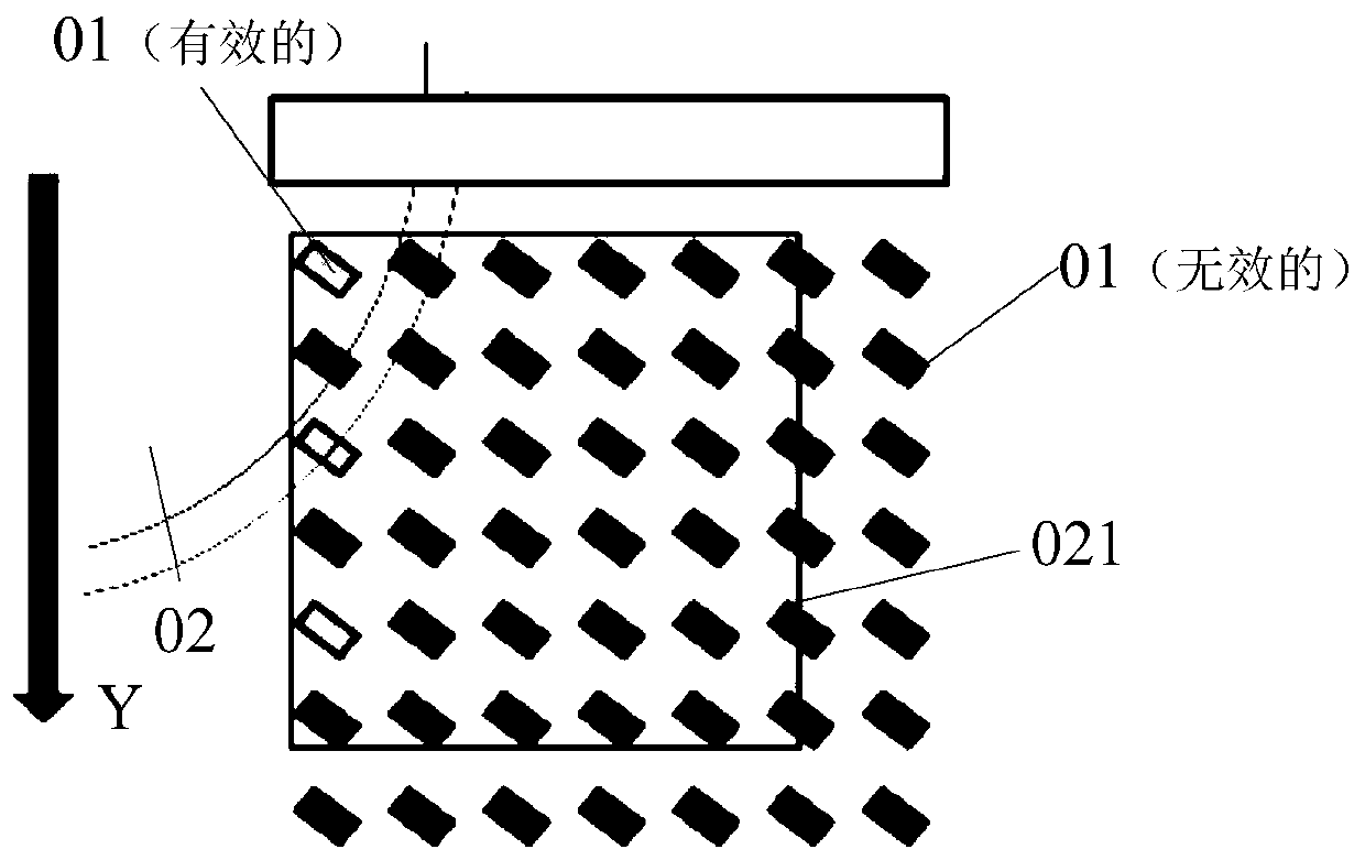
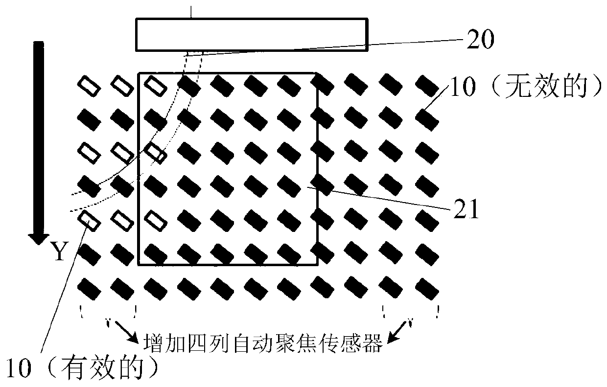
[0027] Step 1: Provide a lithography machine equipped with an autofocus sensor 10. The scanning direction of the lithography machine during lithography is defined as the scanning direction, also defined as the Y direction, and the direction perpendicular to the scanning direction on the horizontal plane is defined as the non-scanning direction , is also defined as the X direction, the arrangement of the autofocus sensors 10 along the non-scanning direction is defined as a row, and the arrangement along the scanning direction is defined as a row, compared with the autofocus sensor in the existing phot...


PUM


Abstract

The invention provides a photoetching method used for alleviating wafer edge defocusing. According to the photoetching method used for alleviating wafer edge defocusing, the column number of automatic focusing sensors in a photoetching machine is increased, when the photoetching machine is used for exposure of an exposure region at the edge of a wafer, the automatic focusing sensor above the exposure region is used for measuring un-scanning direction horizontal value of the exposure region, and realizing compensation of the obtained un-scanning direction horizontal value into edge flatness of the exposure region, so that the exposure region possesses edge flatness of itself obtained via automatic focusing sensor measuring, borrowing of the un-scanning direction horizontal value of a former exposure region in the prior art that is avoided, the difference of the un-scanning direction horizontal value with the Z1 value used in automatic focusing in the exposure region is reduced, wafer edge defocusing is alleviated, and photoetching precision is increased.

Description

technical field [0001] The invention relates to the field of photolithography technology, in particular to a photolithography method for slowing down the defocusing of wafer edges. Background technique [0002] In semiconductor manufacturing technology, it is difficult for the lithography machine to detect and control the edge flatness (leveling value) of the wafer, especially the defocusing (defocus) occurs due to the unobtainable or wrong flatness information of the wafer edge feature area. ), graphic deformation, affecting the electrical performance and yield of the final lithography product. [0003] Exposure is the most important step in the photolithography process. Exposure and imaging are affected by many factors. The energy of exposure and imaging focus shift are particularly important. Imaging focus shift is defocus, and the amount of focus shift is determined by the lithography machine. It is determined by the leveling value detected by the auto focus sensor (AF ...

Claims


Application Information

Patent Timeline
Patent Type & Authority Patents(China)
IPC IPC(8): G03F7/20G03F9/00
CPCG03F7/70466G03F9/7026
Inventor 刘方群朱治国郑海昌
Owner SHANGHAI HUALI MICROELECTRONICS CORP
Why Eureka
Try Eureka