Double-layer PCB

A double-layer, flat part technology, applied in the direction of electrical connection of printed components, printed circuit components, etc., can solve the problems of cabinet performance degradation, moisture intrusion, ugly appearance, etc., and achieve high welding stability and low false soldering rate Effect

Active Publication Date: 2017-08-18
安徽宏鑫电子科技有限公司
View PDF4 Cites 0 Cited by
  • Summary
  • Abstract
  • Description
  • Claims
  • Application Information

AI Technical Summary

Problems solved by technology

The top side welds of the traditional gable roof run through the whole top side, without any surface treatment, the appearance is rather ugly
But the most important problem is that the traditional weld seam structure is single, which leads to the fact that once the weld seam is weakly welded when the cabinet body is corroded by moisture, the external moisture can easily invade the interior of the cabinet body from the position of the weld seam. It makes the actual IP level of the cabinet inconsistent with the marked IP level
Decrease the performance of the cabinet

Method used


Image

  • Double-layer PCB
  • Double-layer PCB

Examples


Embodiment 1

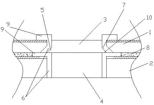
[0019] Such as figure 1 As shown, the embodiment of the present invention includes a first layer of board body 1 and a second layer of board body 2, the first layer of board body 1 is provided with a first via hole 3, and the second layer of board body 2 is provided at a position corresponding to the first via hole 3 There is a second via hole 4, and the junction of the first via hole 3 and the second via hole 4 is provided with a stagnant tin part 5 whose aperture diameter is larger than that of the first via hole 3 and the second via hole 4. The tin stagnation part 5 has at least There is a plane part 10 provided with the conductive material 6 , and the plane of the plane part 10 is parallel to the surface of the board body 1 . To the conductive substance 6 is a conductive copper foil layer. A conductive pad 9 and an insulating layer 8 are arranged between the two-layer board 2 and the side board, and the thickness of the insulating layer 8 is the same as that of the conduc...

Embodiment 2

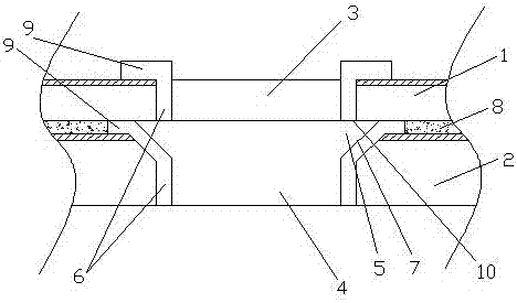
[0021] Such as figure 2 As shown, the embodiment of the present invention includes a first layer of board body 1 and a second layer of board body 2, the first layer of board body 1 is provided with a first via hole 3, and the second layer of board body 2 is provided at a position corresponding to the first via hole 3 There is a second via hole 4, and the junction of the first via hole 3 and the second via hole 4 is provided with a stagnant tin part 5 whose aperture diameter is larger than that of the first via hole 3 and the second via hole 4. The tin stagnation part 5 has at least There is a plane part 10 provided with the conductive material 6 , and the plane of the plane part 10 is parallel to the surface of the board body 1 . To the conductive substance 6 is a conductive copper foil layer. A conductive pad 9 and an insulating layer 8 are arranged between the two-layer board 2 and the side board, and the thickness of the insulating layer 8 is the same as that of the condu...


PUM


Abstract

Provided is a double-layer PCB, which comprises a first layer of board body and a second layer of board body. The first layer of board body is provided with a first via hole; the second layer of board body is provided with a second via hole in the place corresponding to the first via hole; the joint place between the first via hole and the second via hole is provided with a hysteresis tin portion, the diameter of which is larger than that of the first via hole and the second via hole; the hysteresis tin portion is at least internally provided with a plane portion having a conductive material; and the plane where the plane portion locates is parallel to the surface of the first layer of board body. The double-layer PCB has the advantages of low virtual welding rate during wave-soldering process and high welding stability.

Description

technical field [0001] The invention relates to the field of shell structure of a ring network cabinet, in particular to a double-layer PCB. Background technique [0002] The traditional low-voltage cable branch box top adopts a herringbone top, but for a cabinet with a higher IP rating, when the top side welds must be fully welded, it is easy to cause top welding deformation. In addition, with the continuous improvement of people's requirements for the appearance of the cabinet, more and more low-voltage branch boxes are made of stainless steel, which increases the requirements for the appearance of the cabinet during the production process. The top side welds of the traditional gable roof run through the whole top side, without any surface treatment, the appearance is rather ugly. But the most important problem is that the traditional weld seam structure is single, which leads to the fact that once the weld seam is weakly welded when the cabinet body is corroded by moistu...

Claims


Application Information

Patent Timeline
IPC IPC(8): H05K1/11
Inventor 陈世杰
Owner 安徽宏鑫电子科技有限公司
Why Eureka
Try Eureka