

Microelectromechanical system (MEMS) package
A technology of packaging and components, applied in the direction of optical components, semiconductor devices, electrical solid devices, etc., can solve the problem of not being able to manufacture control ICs
Inactive Publication Date: 2017-08-29
AT & S AUSTRIA TECH & SYSTTECHN AKTIENGES
View PDF7 Cites 8 Cited by
- Summary
- Abstract
- Description
- Claims
- Application Information
AI Technical Summary
Problems solved by technology
These further developments relative to the original state lead to the inability to fabricate the control IC on the same substrate as the MEMS part itself
Even with the in
Method used
View moreImage
Smart ImageViewing Examples

Examples
 PUM
 Abstract
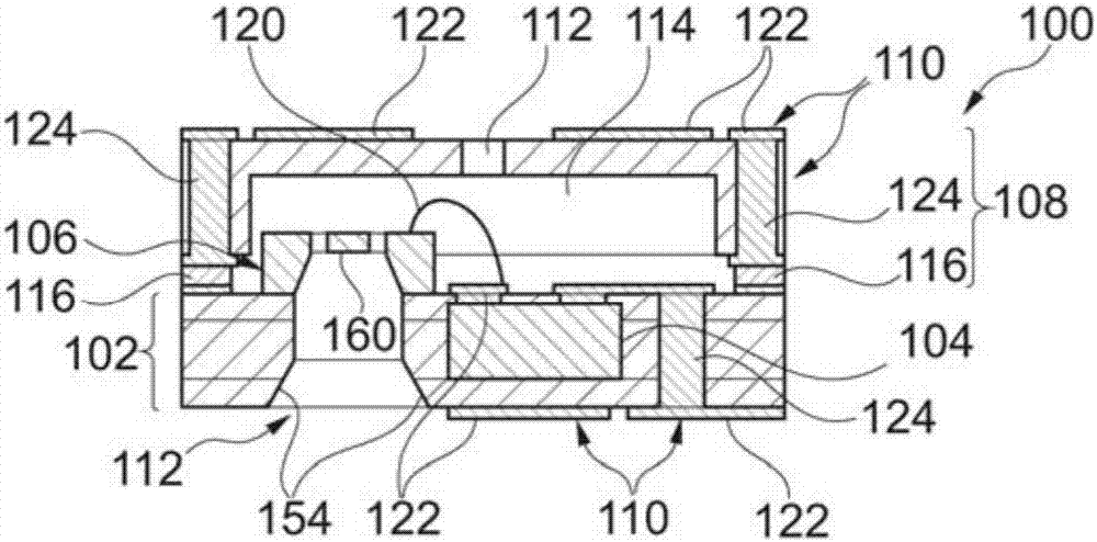
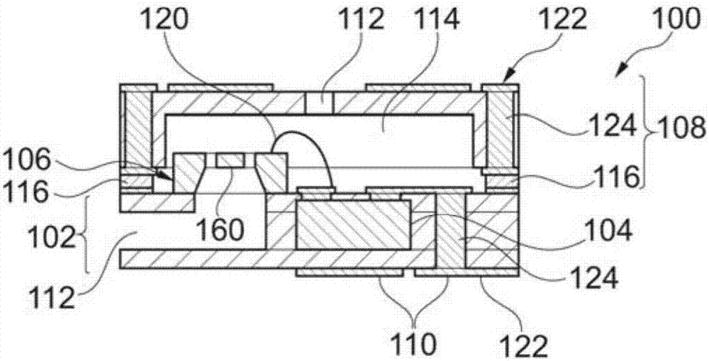
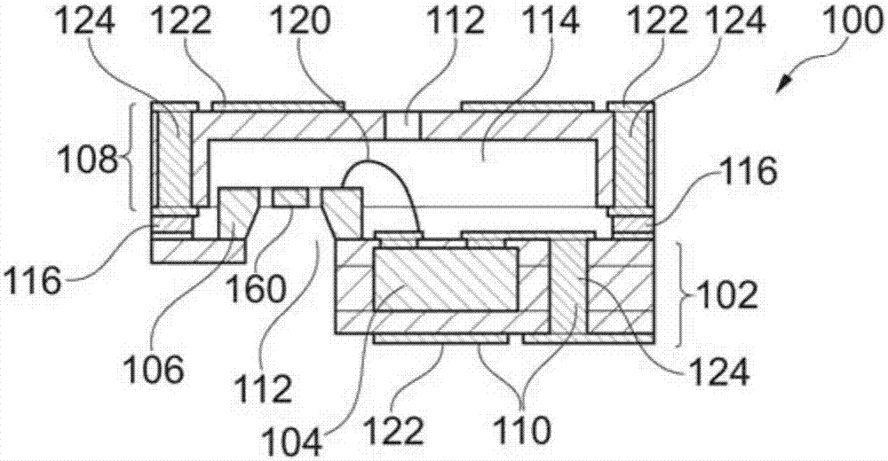
The invention relates to a package comprising a base structure (102) which comprises an electrically insulating material and/or an electrically conductive contact structure (110), an electronic component (104) which is embedded in the base structure (102) or on the base structure (102), a microelectromechanical system (MEMS) component (106) and a cover structure (108) which is mounted on the base structure (102) to at least partially cover the MEMS component (106)
Description
technical field [0001] The invention relates to a package, an arrangement and a method for manufacturing an electronic device. Background technique [0002] Firstly, MEMS components (microelectromechanical systems, micro-electromechanical systems) are fabricated with traditional semiconductor tools. Special requirements regarding eg dimensions, materials, shapes etc. lead to the development of specialized processes. These further developments over the original state resulted in the inability to fabricate control ICs on the same substrate as the MEMS components themselves. Even with the introduction of CMOS-compatible processes (which enabled single-chip MEMS / ICs), the vast majority of MEMS applications separate the sensor / actuator from the control system. With the trend of progress towards smaller form factors and increased efficiency at lower cost, there is room for further developments in view of heterogeneous integration. Contents of the invention [0003] It is an o...
Claims
Login to View More Application Information
Patent Timeline
 IPC IPC(8): B81C1/00B81C3/00B81B7/02H04R19/00H04R19/04
CPCB81B7/02B81C1/0023B81C3/008H04R19/005H04R19/04B81B2201/0257B81B2207/096B81B2207/095H04R2201/003H01L2224/48091H01L2924/15151H01L2924/00014B81B7/0061B81B2207/012B81C2203/0785H04R19/02
Inventor 马库斯·莱特格布尼克·雷诺·贝佐特
Owner AT & S AUSTRIA TECH & SYSTTECHN AKTIENGES