A Novel Polarized Uncooled Infrared Focal Plane Detector and Its Preparation Method

A focal plane detector, uncooled infrared technology, used in instruments, measuring devices, electrical solid devices, etc., can solve the problems of complex optical path system, complex optical components, difficult design, etc., to simplify the optical system and reduce the number of optical components. , to achieve the effect of monolithic integration

Active Publication Date: 2018-09-18
YANTAI RAYTRON TECH
View PDF5 Cites 0 Cited by
  • Summary
  • Abstract
  • Description
  • Claims
  • Application Information

AI Technical Summary

Problems solved by technology

[0004] In addition, in the existing polarization detection system, the polarization element is independent of the detector, and it is necessary to add a polarizer to the lens of the whole machine, or to design a polarization lens. This method is relatively expensive and difficult to design. Large; the polarization information is obtained by rotating the polarization element. The disadvantages of this existing polarization detection system are: the optical elements are complicated, and the optical path system is complicated
The polarization image collected through the combination of polarizer and detector needs to be processed by image fusion algorithm, which is not only complicated but also relatively inaccurate

Method used


Image

  • A Novel Polarized Uncooled Infrared Focal Plane Detector and Its Preparation Method
  • A Novel Polarized Uncooled Infrared Focal Plane Detector and Its Preparation Method
  • A Novel Polarized Uncooled Infrared Focal Plane Detector and Its Preparation Method

Examples


Embodiment 1

[0074] The present invention proposes a novel uncooled infrared focal plane detector pixel structure preparation method, comprising the following steps:

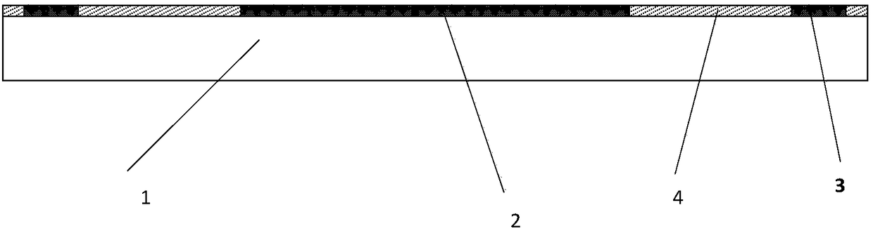
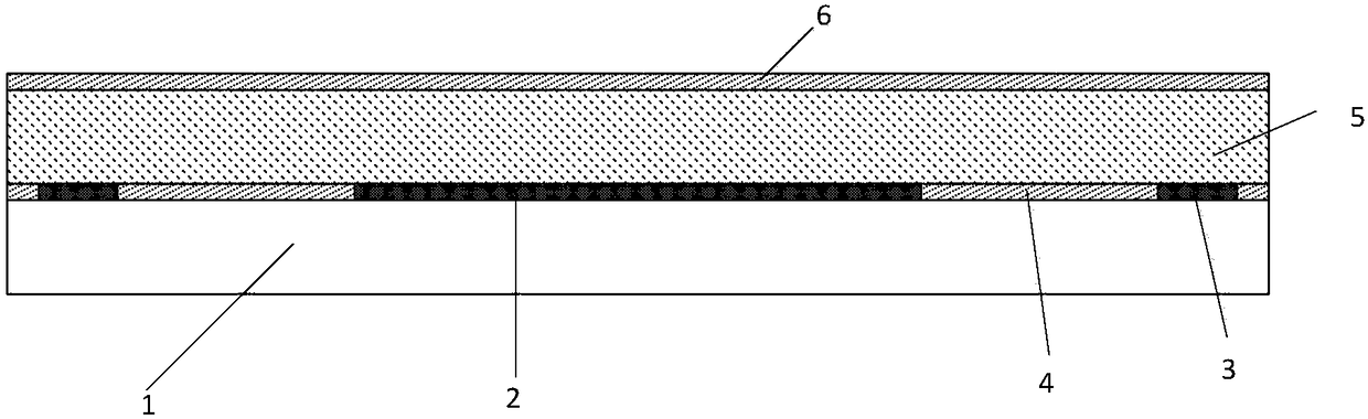
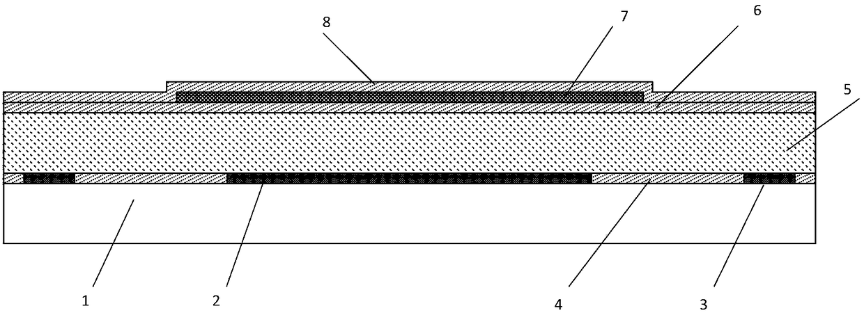
[0075] Step 1: Fabricate a metal reflective layer 2 on the semiconductor base 1 containing the readout circuit; and pattern the metal layer, and the patterned metal reflective layer forms several metal blocks 3; the metal block 3 and the semiconductor base 1 The electrical connection of the readout circuit on the surface; the insulating medium layer 4 is deposited on the patterned metal reflective layer 2; the thickness of the metal reflective layer 2 is The reflective layer metal has a reflectivity of more than 99% for infrared light with a wavelength of 8-14um; the insulating medium layer 4 is a silicon nitride film or a silicon oxide film with a thickness of

[0076] Step 2: sequentially depositing a first sacrificial layer 5, a first supporting layer 6, a heat sensitive layer 7 and a first protective layer 8 on the in...

Embodiment 2

[0087] The difference from Example 1 is that in step 10, when preparing the metal grating structure, a metal thin film is first deposited or sputtered on the grating support layer by physical vapor deposition or sputtering, and then etched by a dry etching process. Eclipse grating graphics, the grating graphics can be straight or curved, such as Figure 10-12 shown, its angle can be changed and is not limited to Figure 10-12 For several types shown in , the interval between adjacent gratings is 10-500 nm.


PUM

PropertyMeasurementUnit
thicknessaaaaaaaaaa
thicknessaaaaaaaaaa
thicknessaaaaaaaaaa

Abstract

The invention relates to a novel polarized uncooled infrared focal plane detector, comprising a semiconductor base, a metal reflection layer, an insulating medium layer, a support layer, a protective layer, a metal electrode layer, and a heat-sensitive layer, wherein the protective layer includes a first protective layer. layer and a second protective layer, the second protective layer is arranged on the thermosensitive layer, the second protective layer is provided with a polarization structure, and the polarization structure includes a grating support layer and is arranged on the grating support layer The metal grating structure adopts the inverted micro-bridge. There is no supporting pier under the micro-bridge, so the structure is not easy to deform; it adopts a three-layer micro-bridge structure, the first layer is an infrared radiation absorption structure, the second layer is a thermal insulation micro-bridge structure, and the third The three layers are polarized structures, which can effectively improve the filling factor of pixels and improve the absorption efficiency of incident infrared radiation; it also relates to a preparation method of a novel polarized uncooled infrared focal plane detector. The two sacrificial layers can be continuously etched, and the wafer surface Very flat.

Description

technical field [0001] The invention belongs to the field of micro-electromechanical system process manufacturing in semiconductor technology, and in particular relates to a novel polarization uncooled infrared focal plane detector and a preparation method thereof. Background technique [0002] The unit of the uncooled infrared focal plane array detector usually adopts a cantilever beam micro-bridge structure, and the micro-bridge support structure is formed by using the sacrificial layer release process, and the heat-sensitive material on the support platform is connected to the substrate readout circuit through the micro-bridge. Now the requirements for the resolution of the detector are getting higher and higher, and the requirements for the array are getting bigger and bigger. If the size of the chip remains the same, the pixels will become smaller and smaller, and the requirements for the flatness of the pixels will be higher and higher; both sides The micro-bridge stru...

Claims


Application Information

Patent Timeline
Patent Type & Authority Patents(China)
IPC IPC(8): B81B7/00B81B7/02B81C1/00
CPCB81B7/0009B81B7/02B81B2201/02B81C1/0038B81C1/00388B81C1/00396
Inventor 邱栋杨水长王鹏王宏臣陈文礼
Owner YANTAI RAYTRON TECH
Why Eureka
Try Eureka