Microstructure substrate and manufacturing method thereof and display device

A manufacturing method and technology for a display device, which are applied in the directions of ion implantation, plating, coating, instruments, etc., can solve the problems of blurred image quality and reduced panel resolution, and achieve the effect of improving the impact of image quality and reducing the degree of blurring.

Active Publication Date: 2017-09-05
WUHAN CHINA STAR OPTOELECTRONICS TECH CO LTD
View PDF1 Cites 2 Cited by
  • Summary
  • Abstract
  • Description
  • Claims
  • Application Information

AI Technical Summary

Problems solved by technology

[0002] At present, the anti-glare (anti-glare) treatment method commonly used by panel manufacturers is to prepare uneven topography on the surface of glass or plastic substrates. However, after this anti-glare substrate is bonded to a high-resolution substrate, the displayed image quality will be blurred. Causes a decrease in the actual resolution of the panel

Method used


Image

  • Microstructure substrate and manufacturing method thereof and display device
  • Microstructure substrate and manufacturing method thereof and display device
  • Microstructure substrate and manufacturing method thereof and display device

Examples


Embodiment Construction

[0015] The following will clearly and completely describe the technical solutions in the embodiments of the present invention with reference to the accompanying drawings in the embodiments of the present invention. Obviously, the described embodiments are only some, not all, embodiments of the present invention. Based on the embodiments of the present invention, all other embodiments obtained by persons of ordinary skill in the art without making creative efforts belong to the protection scope of the present invention.

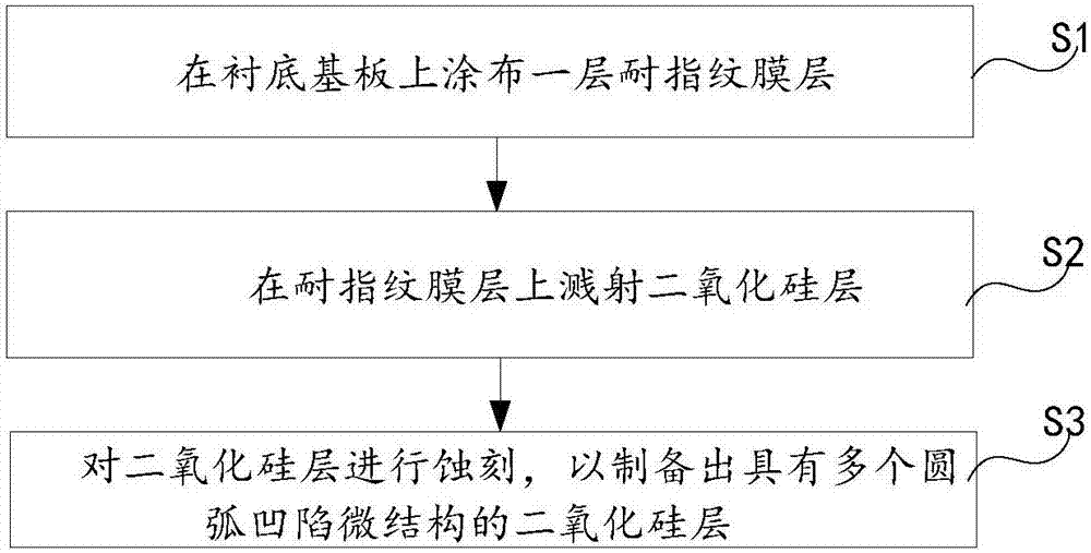
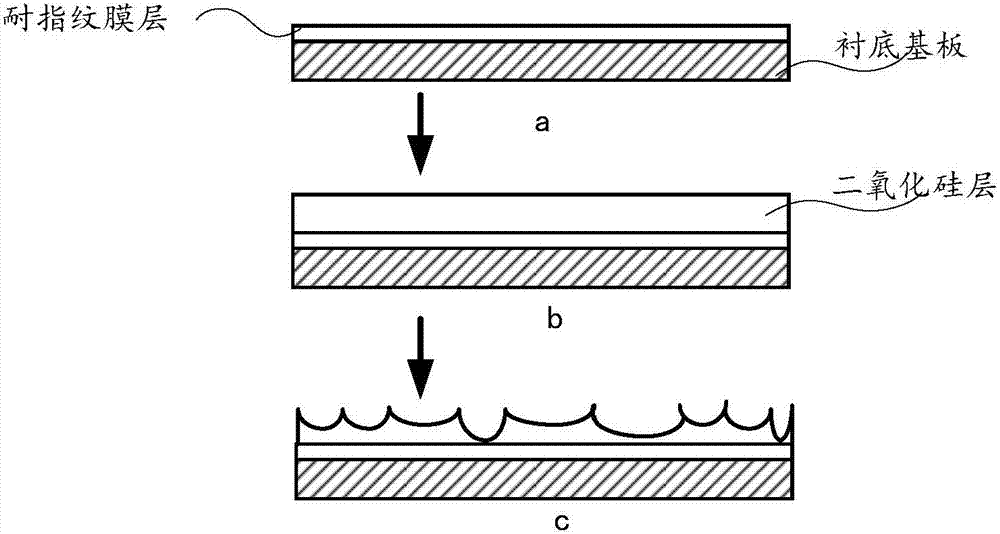
[0016] see figure 1 , figure 1 It is a schematic flow chart of an embodiment of the manufacturing method of the microstructure substrate of the present invention, figure 2 It is a structural schematic diagram of an embodiment of the preparation process of the microstructure substrate of the present invention, and the method includes the following steps:

[0017] S1, coating a layer of anti-fingerprint film on the base substrate.

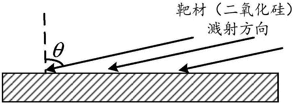
[0018] see further figu...


PUM

PropertyMeasurementUnit
thicknessaaaaaaaaaa
widthaaaaaaaaaa
thicknessaaaaaaaaaa

Abstract

The invention discloses a microstructure substrate and a manufacturing method thereof and a display device. The method comprises the steps that a fingerprint-resistant film layer is coated on an underlying substrate; a silicon dioxide layer is sputtered on the fingerprint-resistant film layer; and the silicon dioxide layer the etched so as to prepare the silicon dioxide layer having multiple arc concave microstructures. With application of the mode, the influence of the microstructures on the high-resolution panel picture quality can be improved, the blur degree of the picture quality can be reduced and the substrate is enabled to be applied to the high-resolution panel.

Description

technical field [0001] The invention relates to the field of display technology, in particular to a microstructure substrate, a manufacturing method, and a display device. Background technique [0002] At present, the anti-glare (anti-glare) treatment method commonly used by panel manufacturers is to prepare uneven topography on the surface of glass or plastic substrates. However, after this anti-glare substrate is bonded to a high-resolution substrate, the displayed image quality will be blurred. Causes a drop in the actual resolution of the panel. Therefore, this kind of anti-glare substrate is only used in panels that do not require high resolution in most cases. Contents of the invention [0003] The invention provides a microstructure substrate, a manufacturing method, and a display device, which can improve the influence of the microstructure on the image quality of a high-resolution panel, reduce the blurring degree of the image quality, and make it possible for th...

Claims


Application Information

Patent Timeline
Patent Type & Authority Applications(China)
IPC IPC(8): G02B5/02G02B1/18
CPCG02B5/0221G02B5/0268G02B1/18C23C14/10C23C14/225C23C14/34C23C14/5873
Inventor 杨勇
Owner WUHAN CHINA STAR OPTOELECTRONICS TECH CO LTD
Why Eureka
Try Eureka