Semiconductor device

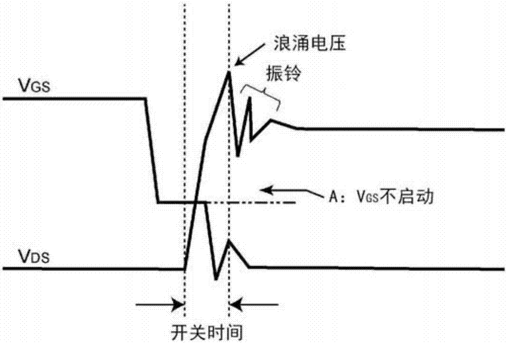
A semiconductor and substrate technology, applied in semiconductor devices, electrical components, circuits, etc., can solve the problems of reducing surge voltage, slowing switching speed, increasing switching loss, etc., to prevent the increase of switching loss and speed up switching speed , The effect of reducing the surge voltage

Active Publication Date: 2017-09-05
SHINDENGEN ELECTRIC MFG CO LTD
View PDF5 Cites 4 Cited by
  • Summary
  • Abstract
  • Description
  • Claims
  • Application Information

AI Technical Summary

Problems solved by technology

[0007] However, once a high-resistance shield electrode is used as the shield electrode as described above, in the second half of the switching cycle, since a potential difference occurs along the wiring of the shield electrode, the gate-source capacitance C GS (Refer to Figure 20, it is the same situation in Figure 2) Gate voltage V GS It will rise suddenly, so there is a problem of easy operation error (self-turn-on (Self Turn-On)) (refer to symbol A in Figure 2(b))
In addition, due to the slow switching speed (see Figure 2(b)), there is also the problem of increased switching loss
[0008] On the other hand, if a low-resistance shield electrode is used as the shield electrode (see Fig. 3(a)), since the potential change of the drain electrode cannot be moderated when the switch is turned off, it is impossible to obtain ringing suppression at the same time. Effect of reducing surge voltage (see Figure 3(b))

Method used


Image

  • Semiconductor device
  • Semiconductor device
  • Semiconductor device

Examples


Embodiment approach 1

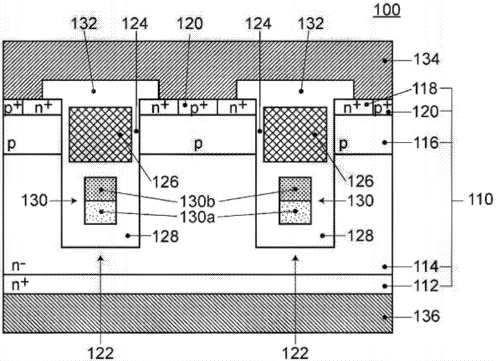
[0045] 1. Semiconductor device

[0046] The semiconductor device related to Embodiment 1, as shown in FIG. The adjacent n-type drift region (first conductivity type drift region) 114, the p-type base region (second conductivity type base region) 116 adjacent to the n-type drift region 114, and the p-type base region An n+ type source region (first conductivity type source region) 118 adjacent to the pole region 116; a trench 122, formed in the semiconductor base 110, having a groove bottom adjacent to the n-type drift region 114, and The sidewall adjacent to the p-type base region 116 and the n-type drift region 114 is formed in a stripe shape when viewed from the plane; The gate insulating film 124 is opposite to the p-type base region 116; the shielding electrode 130 is arranged in the trench 122, and is located between the gate electrode 126 and the bottom of the trench 122; the electrically insulating region in the trench 122 128, extending between the gate electrode 126...

Embodiment approach 2

[0088] The semiconductor device 101 according to the second embodiment basically has the same configuration as the semiconductor device 100 according to the first embodiment, but differs from the semiconductor device 100 according to the first embodiment in the configuration of the shield electrode. That is, if Figure 9 As shown, in the semiconductor device 102 according to Embodiment 2, the high-resistance region 130a and the low-resistance region 130b are made of different materials, and the resistivity of the material constituting the low-resistance region 130b is lower than that of the material constituting the high-resistance region 130a. The resistivity of the material (see Figure 9 ).

[0089] As a material constituting the high-resistance region 130a, for example, high-resistance polysilicon formed by CVD can be used. In addition, as a material constituting the low-resistance region 130b, for example, a metal with a high melting point (eg, W, Mo, Ta, Nb, etc.) and ...

Embodiment approach 3

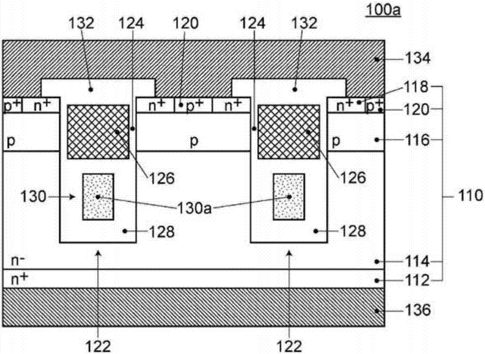
[0093] The semiconductor device according to the third embodiment basically has the same configuration as the semiconductor device 100 according to the first embodiment, but differs from the semiconductor device 100 according to the first embodiment in the configuration of the shield electrode. That is, if Figure 10 As shown, in the semiconductor device 102 according to the third embodiment, the high-resistance region 130 a and the low-resistance region 130 b are located at positions separated from each other via the electrically insulating region 128 .

[0094] The interval between the high-resistance region 130a and the low-resistance region 130b can be appropriately set, for example, it can be set to 1 μm.

[0095] In this way, although the semiconductor device 102 according to the third embodiment is different from the semiconductor device 100 according to the first embodiment in the configuration of the shield electrode, it has the high resistance region 130a located on ...


PUM


Abstract

A semiconductor device 100 comprising: gate electrodes 126 arranged inside trenches 122 and facing p-type base regions 116, via gate insulating films 124, in a side wall section; shield electrodes 130 arranged inside the trenches 122 and positioned between the gate electrodes 126 and the bottom of the trenches 122; electrical insulation regions 128 inside the trenches 122, spreading between the gate electrodes 126 and the shield electrodes 130 and spreading along the side wall and bottom of the trenches 122 and isolating the shield electrodes 130 from the side walls and bottom; and a source electrode 134 electrically connected to n+ source regions 118 and the shield electrodes 130. The shield electrodes 130 have a high-resistance region 130a positioned on an n+ drain region 112 side and a low-resistance region 130 positioned on the gate electrode 126 side. As a result, ringing and surge voltage can be suppressed, malfunctions can be suppressed, and increase in switching loss can be prevented.

Description

technical field [0001] The present invention relates to semiconductor devices. Background technique [0002] Conventionally, a semiconductor device having a structure called a gate shield (Shield Gate) has been widely known (for example, refer to Patent Document 1). As shown in FIG. 20(a), a conventional semiconductor device 900 includes: a semiconductor base 910 including: an n+ type drain region 912, an n-type drift region 914, a p-type base region 916, and an n+ type source region 918 Trench (Trench) 922, has: be formed in semiconductor substrate 910, and the trench bottom adjacent to n-type drift region 914, and adjacent to p-type base region 916 and n-type drift region 914 connected sidewall, and formed in a stripe (Stripe) shape from a plan view; the gate electrode 926 is arranged in the trench 922, and is opposed to the p-type base region 916 via the insulating film 924 at the sidewall portion; The shielding electrode 930 is arranged in the trench 922 and is located...

Claims


Application Information

Patent Timeline
Patent Type & Authority Applications(China)
IPC IPC(8): H01L29/78
CPCH01L29/404H01L29/407H01L29/435H01L29/66734H01L29/7813H01L29/1095H01L29/36H01L29/4236H01L29/7811
Inventor 岸雅人渡边祐司竹森俊之穴泽健夫秋元俊孝
Owner SHINDENGEN ELECTRIC MFG CO LTD
Why Eureka
Try Eureka