

Flexible display mother board and fabrication method and cutting method thereof
A flexible display and cutting method technology, applied in semiconductor/solid-state device manufacturing, photovoltaic power generation, electrical components, etc., can solve the problem of large consumables, and achieve the effect of reducing consumables
- Summary
- Abstract
- Description
- Claims
- Application Information
AI Technical Summary
Problems solved by technology
Method used
Image

Examples
Embodiment 1
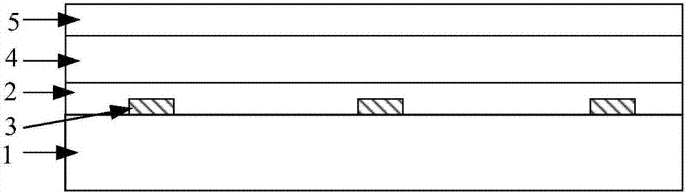
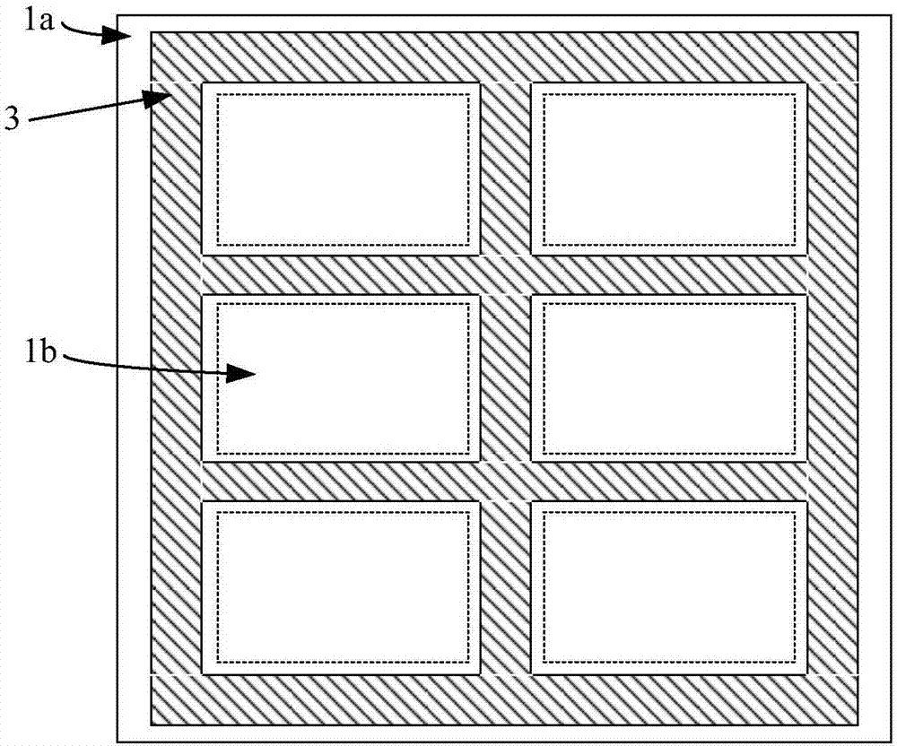
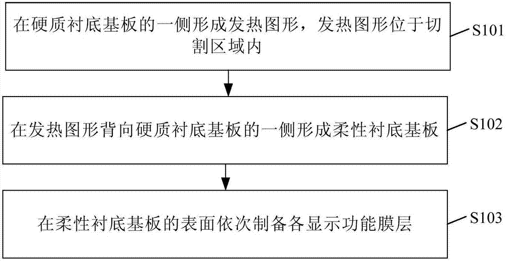
[0040] figure 1 It is a schematic structural diagram of a flexible display motherboard provided by Embodiment 1 of the present invention, figure 2 for figure 1 The top view of the flexible display motherboard shown, such as figure 1 with figure 2 As shown, the flexible display motherboard includes: a hard base substrate 1 and a flexible base substrate 2 located on one side of the hard base substrate. The flexible base substrate 2 is divided into a cutting area 1a and a non-cutting area 1b. A heating pattern 3 is formed on the side of the base substrate 1 facing the flexible substrate 2 and corresponding to the cutting area 1a, and the heating pattern 3 is used to generate heat to cut the cutting area 1a.
[0041] Optionally, the heat-generating pattern 3 is made of an electro-heating material, and the heat-generating pattern 3 generates heat after an electric current is applied. Preferably, the material of the heating pattern 3 is a material with high electrothermal conv...
Embodiment 2
[0058] Figure 4 A schematic structural diagram of a flexible display motherboard provided in Embodiment 2 of the present invention, as shown in Figure 4 As shown, the difference from the first embodiment above is that the heating pattern 3 in this embodiment is located inside the flexible substrate 2 .
[0059] In this embodiment, considering that the thickness of the flexible substrate 2 is relatively thick, the cutting of the flexible substrate 2 requires more energy. By placing the heating pattern in the flexible substrate 2, the actual cutting thickness of the heating pattern can be reduced, thereby effectively reducing the energy required for the cutting process. Preferably, the distance between the heating pattern 3 and the upper and lower surfaces of the flexible substrate 2 is equal, and at this time, the energy required for cutting the flexible substrate 2 is minimum.
[0060] Figure 5 It is a schematic diagram of the heating pattern located in the flexible subs...
Embodiment 3
[0072] Figure 7 A schematic structural diagram of a flexible display motherboard provided in Embodiment 3 of the present invention, as shown in Figure 7 As shown, different from the first and second embodiments above, the heating pattern 3 in this embodiment is located on the side of the flexible substrate 2 facing away from the hard substrate 1 .
[0073] In this embodiment, it is considered that several display function layers 4 are generally provided in the flexible display motherboard for displaying. If the heat generation pattern is too far away from the display function layer 4, the display function layer 4 cannot be cut. For this reason, in this embodiment, the heating pattern 3 is arranged on the side of the flexible substrate facing away from the hard substrate.
[0074] In addition, considering the thickness of the flexible substrate 2 is relatively thick, the cutting of the flexible substrate 2 requires more energy. If the heating pattern 3 is too far away from t...
PUM
 Abstract
Description
Claims
Application Information