Array substrate, display panel and display device

A technology for array substrates and display panels, applied in identification devices, static indicators, instruments, etc., can solve the problems of large space, increase the thickness of the display screen, and the large size of the lower frame of the touch display screen, so as to achieve narrow frame, The effect of reducing the number

Active Publication Date: 2017-09-12
XIAMEN TIANMA MICRO ELECTRONICS
View PDF7 Cites 38 Cited by
  • Summary
  • Abstract
  • Description
  • Claims
  • Application Information

AI Technical Summary

Problems solved by technology

[0004] In the prior art, the touch display screen is used to realize the electrical connection between the data pins of the control chip and the demultiplexer. The first wiring is used to realize the electrical connection between the touch electrode drive circuit and the touch electrode signal selection circuit. Two wires, since the control chip, touch electrode drive circuit, touch electrode signal selection circuit and demultiplexer are arranged in sequence along the edge of the display screen to the direction of the display area, therefore, the first wire and the second wire There is an overlapping part between the first trace and the second trace to be insulated, which will increase the thickness of the display
In addition, the control chip of the touch screen needs to be specially provided with touch signal control pins, and the larger touch electrode signal selection circuit requires a larger space to set up, resulting in a larger size of the lower frame of the touch screen

Method used


Image

  • Array substrate, display panel and display device
  • Array substrate, display panel and display device
  • Array substrate, display panel and display device

Examples


Embodiment Construction

[0024] In order to further explain the technical means and effects of the present invention to achieve the intended purpose of the invention, the specific implementation, structure, Features and their functions are described in detail below.

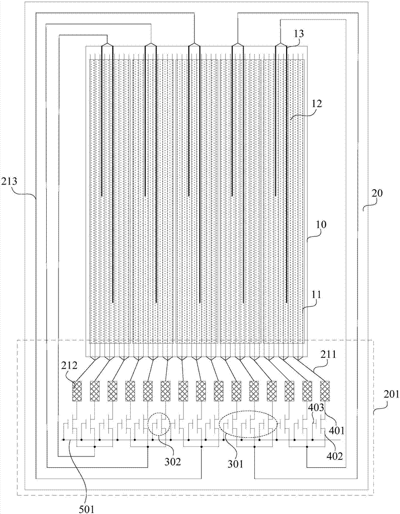
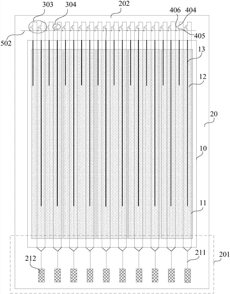
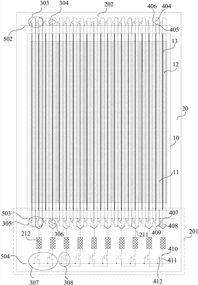
[0025] An embodiment of the present invention provides an array substrate, and the array substrate includes a display area and a non-display area arranged around the display area;

[0026] The display area includes a plurality of data lines and a plurality of first touch electrodes;

[0027] A plurality of data signal lines and a plurality of discrete pads are arranged in the first non-display area on one side of the display area;

[0028] Each of the data signal lines is connected to at least one of the data lines, each of the pads is electrically connected to one of the data signal lines, and at least one of the pads is electrically connected to one of the first touch electrodes;

[0029] The pads are used to provide data signals for...


PUM


Abstract

The invention discloses an array substrate, a display panel and a display device. The array substrate comprises a display region and non-display regions arranged around the display region, wherein the display region comprises multiple data wires and multiple first touch electrodes; multiple data signal wires and multiple separate bonding pads are arranged in the first non-display region located on one side of the display region; each data signal wire is connected with at least one data wire; each bonding pad is electrically connected with one data signal wire; at least one bonding pad is electrically connected with one first touch electrode; the bonding pads are used for providing data signals for the data wires in a display stage and providing touch signals for the first touch electrodes in a touch stage. According to the array substrate provided by the invention, the bonding pads can provide corresponding signals in different stages, thus realizing time multiplexing of the bonding pads and reducing the quantity of the bonding pads; furthermore, no other functional circuits are arranged between the bonding disks and the data wires as well as the bonding disks and the touch electrodes, and narrowing of a lower rim of the display device can be realized favorably.

Description

technical field [0001] Embodiments of the present invention relate to display technologies, and in particular to an array substrate, a display panel and a display device. Background technique [0002] The addition of the touch function in the display screen enriches the way of interaction between the user and the electronic device. The touch display screen is favored by more and more users and is widely used in various electronic devices. [0003] In the prior art, a touch display screen includes a display area and a non-display area arranged around the display area. A plurality of touch electrodes and a plurality of data lines are arranged in the display area, and a control chip and a touch electrode drive circuit are arranged in the non-display area. , a touch electrode signal selection circuit and a multiplexer. In the display stage, the control chip transmits the data driving signal to the demultiplexer through the data pin, and then the demultiplexer processes the data...

Claims


Application Information

Patent Timeline
Patent Type & Authority Applications(China)
IPC IPC(8): G09F9/00G02F1/1333G06F3/041
CPCG02F1/13338G06F3/0412G09F9/00H01L2224/16227G06F3/04164G06F3/0446G06F3/0445H01L27/124H01L24/16H01L2224/16145H01L2224/06155H01L24/06G02F1/13458G02F1/13454G09G2300/0408G02F1/13456G02F1/133388
Inventor 潘朝煌曹兆铿周志伟
Owner XIAMEN TIANMA MICRO ELECTRONICS
Why Eureka
Try Eureka