Asymmetric through hole printed circuit board

A printed circuit board, asymmetric technology, applied in the directions of printed circuits, printed circuits, printed circuit components, etc., can solve the problems of large stability and heavy workload, and achieve good impedance continuity and reduce interference. Effect

Active Publication Date: 2017-09-12
安徽宏鑫电子科技有限公司
View PDF5 Cites 4 Cited by
  • Summary
  • Abstract
  • Description
  • Claims
  • Application Information

AI Technical Summary

Problems solved by technology

However, the existing method has a huge workload for the designer during the design process. In actual production, even if the theory can be qualified, there are still big problems in the stability after productization.

Method used


Image

  • Asymmetric through hole printed circuit board
  • Asymmetric through hole printed circuit board

Examples


Embodiment Construction

[0018] The present invention will be described in further detail below in conjunction with the accompanying drawings.

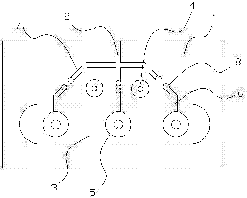
[0019] Such as figure 1 , figure 2 As shown, the embodiment of the present invention includes a base layer 1, a differential signal line 2, an anti-pad 3, and a ground via 4 are arranged on the base layer 1, three signal vias 5 are arranged on the anti-pad 3, and three signal vias 5 are provided on the anti-pad 3. Each of the holes 5 is provided with a transmission signal line 6, and the end of the transmission signal line 6 is provided with a connection pad 8, and one end of the differential signal line 2 is bifurcated into three opposite reception signal lines 7, and the end of the reception signal line 7 is provided with a There are connection pads 8 , and ground vias 4 are provided between adjacent transmission signal lines 6 , and only two signal vias 5 are connected to the differential signal lines 2 by welding the connection pads 8 . Ground vias 4 a...


PUM


Abstract

The invention relates to an asymmetric through hole printed circuit board. The asymmetric through hole printed circuit board comprises a base layer, wherein the base layer is provided with a difference signal wire, an anti-pad and grounding through holes, the anti-pad is provided with three signal through holes, the three signal through holes are respectively provided with a transmission signal wire, end portions of the transmission signal wires are provided with connection pads, one end of the difference signal wire is bifurcated to form three opposite reception signal wires, end portions of the reception signal wires are provided with the connection pads, the grounding through holes are arranged between the adjacent transmission signal wires, and only two of the signal through holes are communicated with the difference signal wires through welding of the connection pads. The asymmetric through hole printed circuit board is advantaged in that good impedance continuity is realized, interference reduction is realized, and adjustment on signal through hole connection modes can be realized according to field demands.

Description

technical field [0001] The invention relates to the field of PCB structures, in particular to an asymmetric via-hole printed circuit board. Background technique [0002] In high-speed PCB design, seemingly simple vias often bring great negative effects to circuit design. In order to reduce the adverse effects caused by the parasitic effects of vias, the existing vias are designed in the following ways: first, consider the cost and signal quality, choose a reasonable size vias, the current technical conditions Under the circumstances, it is difficult to use smaller-sized vias. For power or ground vias, you can consider using larger-sized vias to reduce impedance; Two kinds of parasitic parameters; third, try not to change the layer of the signal trace on the PCB, that is to say, try not to use unnecessary vias; fourth, the pins of the power supply and ground should be drilled through holes nearby, and the vias and The shorter the leads between the pins, the better, because ...

Claims


Application Information

Patent Timeline
Patent Type & Authority Applications(China)
IPC IPC(8): H05K1/02
CPCH05K1/0218H05K1/0251H05K2201/09627
Inventor 陈世杰
Owner 安徽宏鑫电子科技有限公司
Why Eureka
Try Eureka