

Method for optimizing differential via hole impedance, circuit board, equipment and storage medium
A differential via impedance, printed circuit board technology, applied in the direction of printed circuit, printed circuit manufacturing, electrical components, etc., can solve the problems of complex board manufacturing process, failure to meet design requirements, increase cost, etc., to improve link Impedance continuity, optimized via impedance, and the effect of reducing signal reflection
- Summary
- Abstract
- Description
- Claims
- Application Information
AI Technical Summary
Problems solved by technology
Method used
Image

Examples
Embodiment 1
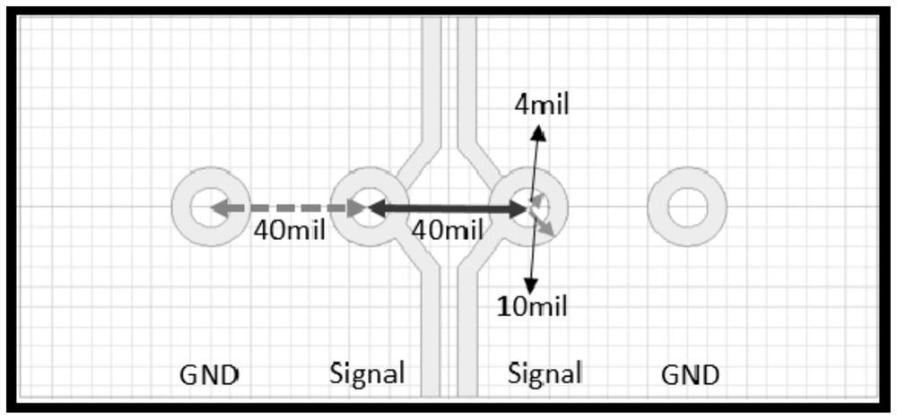
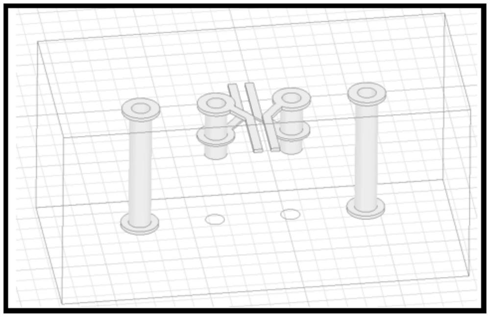
[0034] In order to further illustrate the design method of the present invention, a specific via is taken as an example to describe in detail, as figure 1 The via design of a PCIe Gen4 link is given, in which the radius of the signal hole is 4mil, and the radius of the via pad (via pad) is 10mil. The signal traces on the via hole are changed from layer L1 to layer L5. Such as figure 2 A three-dimensional diagram of the via design of a PCIe Gen4 link in China is given. The target controlled impedance of the vias is 85ohm±2ohm.
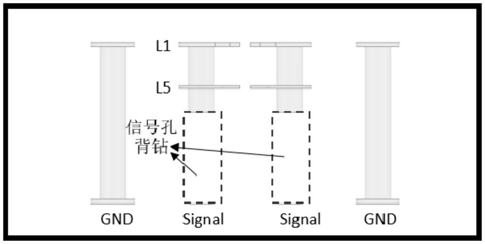
[0035] Due to the high signal rate, the via hole has a 51mil via stub (via stub), so the signal hole is back-drilled, and the back-drilling depth is 41mil, such as image 3 The back-drilling of the vias is given, and only the back-drilling is performed for the signal holes. Such as Figure 4 It is a schematic diagram of a PCIe Gen4 via anti-pad design in Embodiment 1 of the present invention. Figure 4 The picture above is the anti-pad design of ...
Embodiment 2
[0062] Based on a method for optimizing differential via impedance proposed in Embodiment 1 of the present invention, Embodiment 2 of the present invention also proposes a printed circuit board, which is processed by a method for optimizing differential via impedance; Both the signal hole and the ground hole of the circuit board are back-drilled; and the depth of the back-drilled ground hole is not greater than the depth of the back-drilled signal hole.
[0063] Before performing the back drilling, calculate the thickness of the via stub according to the signal trace and the thickness of the printed circuit board; determine the depth of the signal hole back drilling according to the thickness of the via stub; according to the depth of the signal hole back drilling Depth determines the depth of the backdrilling of the ground hole;
[0064] The method of calculating the thickness of the via stub according to the signal trace and the thickness of the printed circuit board is: the...
Embodiment 3
[0072] Based on a method for optimizing differential via impedance proposed in Embodiment 1 of the present invention, Embodiment 3 of the present invention also proposes a differential via impedance optimization device for printed circuit boards, including:
[0073] memory for storing computer programs;
[0074] The processor is configured to implement the steps of a method for optimizing differential via impedance when executing the computer program.
[0075] Both the signal hole and the ground hole of the printed circuit board are back-drilled; and the depth of the back-drilled ground hole is not greater than the depth of the back-drilled signal hole.
[0076] Before performing the back drilling, calculate the thickness of the via stub according to the traces of the signal and the thickness of the printed circuit board; determine the depth of the signal hole back drilling according to the thickness of the via stub; according to the depth of the signal hole back drilling Dep...
PUM
 Abstract
Description
Claims
Application Information