Differential signal via hole and coupling capacitor impedance continuity design method, pcb board

A differential signal, coupling capacitor technology, applied in printed circuits, electrical components, circuit devices, etc., can solve problems such as impedance discontinuity, and achieve the effect of avoiding excessive impedance, highlighting substantive characteristics, and wide application prospects.

Active Publication Date: 2022-05-31
SUZHOU METABRAIN INTELLIGENT TECH CO LTD
View PDF0 Cites 0 Cited by
  • Summary
  • Abstract
  • Description
  • Claims
  • Application Information

AI Technical Summary

Problems solved by technology

If the distance between the via hole and the coupling capacitor is relatively long, it will lead to the problem of discontinuity in multiple impedances. The present invention provides a method for designing the impedance continuity of the differential signal via hole and the coupling capacitor, and a PCB board.

Method used


Image

  • Differential signal via hole and coupling capacitor impedance continuity design method, pcb board
  • Differential signal via hole and coupling capacitor impedance continuity design method, pcb board
  • Differential signal via hole and coupling capacitor impedance continuity design method, pcb board

Examples


Embodiment Construction

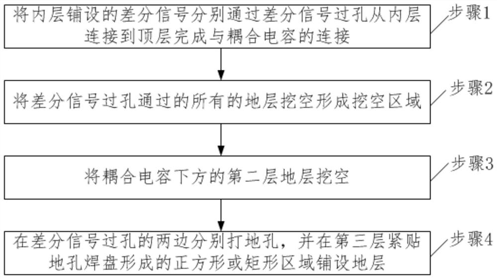
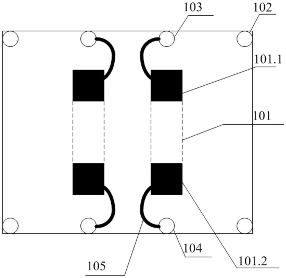
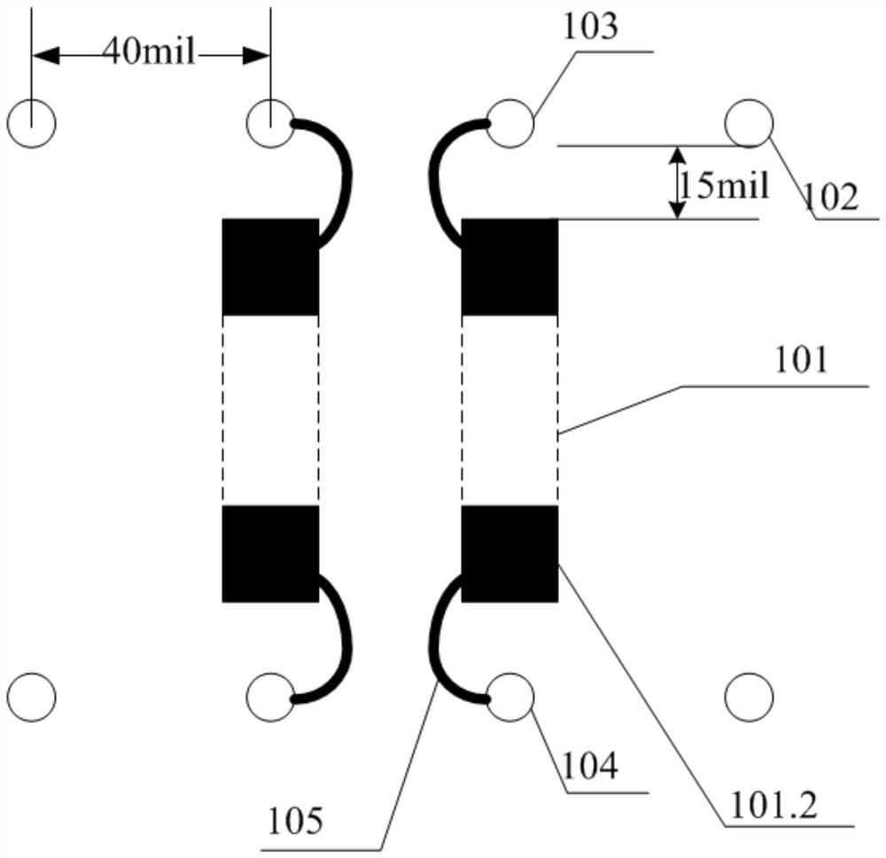
[0060] Avoid the problem of small impedance caused by not hollowing out the reference ground layer of the coupling capacitor and directly hollowing out the adjacent ground layer.

[0064] The component placement attribute is obtained, and the coupling capacitor 101 is placed on the top layer according to the placement attribute.

[0067] The impedance discontinuities of the signal vias and the coupling capacitors are combined into a design, which reduces the discontinuity of the discontinuities.

[0068] In some embodiments, the steps of hollowing out all the ground layers through which the differential signal vias pass to form a hollowed-out area include:

[0070] In some embodiments, the step of hollowing out the second layer of formation below the coupling capacitor includes:

[0071] As shown in FIG. 4, the pad area of ​​the coupling capacitor is hollowed out in the second ground layer; wherein, the coupling capacitor is hollowed out in the second ground layer

[0073] In some ...


PUM


Abstract

The invention provides a method for designing the impedance continuity of differential signal vias and coupling capacitors, and a PCB board. The method includes the following steps: connecting the differential signals laid on the inner layer from the inner layer to the top layer through the differential signal vias to complete and couple Connection of capacitors; Hollow out all the strata through which the differential signal vias pass to form a hollowed out area; Hollow out the second layer of stratum below the coupling capacitor; Drill ground holes on both sides of the differential signal vias, and in the third layer Lay the ground plane next to the square or rectangular area formed by the pad of the ground hole. It avoids the problem of small impedance caused by not hollowing out the capacitance reference formation and the large impedance caused by directly hollowing out the adjacent formation, and greatly optimizes the impedance continuity of the differential signal link with coupling capacitance. Combining the impedance discontinuities of signal vias and coupling capacitors into one design reduces the number of discontinuities and improves signal integrity.

Description

Differential signal via and coupling capacitor impedance continuity design method, PCB board technical field The present invention relates to PCB board wiring impedance continuity design technical field, be specifically related to a kind of differential signal via and Coupling capacitor impedance continuity design method, PCB board. Background technique In the field of electronic design, the circuit board is the physical carrier of all electronic design content, so the intention of electronic design All are implemented through circuit boards, so circuit board design is an indispensable part of any electronic device. [0003] The circuit board design is mainly divided into two parts, signal design and power design. The power supply is designed for the entire board Design basis, all chips need to have a stable power supply to work properly. Signal design is the soul of circuit board design, The realization of various functions needs to be controlled by signals, and t...

Claims


Application Information

Patent Timeline
Patent Type & Authority Patents(China)
IPC IPC(8): H05K3/00H05K1/02
CPCH05K3/0002H05K3/0044H05K1/0251H05K1/025
Inventor 李德恒
Owner SUZHOU METABRAIN INTELLIGENT TECH CO LTD
Why Eureka
Try Eureka