Fault-based three-dimensional optical on-chip network architecture, communication method and optical router

An optical-on-chip network and communication method technology, which is applied to architectures with a single central processing unit, instruments, and general-purpose stored-program computers, can solve problems such as uneven distribution of vertical interconnect lines, achieve good scalability, and control the overall Effects of energy consumption and efficient communication

Active Publication Date: 2017-09-29
XIDIAN UNIV
View PDF5 Cites 2 Cited by
  • Summary
  • Abstract
  • Description
  • Claims
  • Application Information

AI Technical Summary

Problems solved by technology

[0005] The purpose of the present invention is to provide a three-dimensional optical on-chip network architecture, communication method and optical router based on the layer fault mechanism to solve the problem of uneven distribution of vertical interconnection lines under the high-level interconnection mechanism between layers in the prior art

Method used


Image

  • Fault-based three-dimensional optical on-chip network architecture, communication method and optical router
  • Fault-based three-dimensional optical on-chip network architecture, communication method and optical router
  • Fault-based three-dimensional optical on-chip network architecture, communication method and optical router

Examples


Embodiment 1

[0024] Existing 3D optical on-chip networks using low-order vertical interconnection lines cannot fully utilize the high bandwidth advantages of 3D networks, which can easily lead to vertical blocking problems, while existing 3D optical on-chip networks using interlayer high-order interconnection mechanisms The layout method adopted by the network will lead to uneven distribution of vertical interconnection lines, which will destroy the regularity of the network and limit the expansion of the network; it will also cause serious heat dissipation problems; in addition, the existing high-level interconnection between layers The insertion loss of high-end optical routers is large, which can easily lead to an increase in network energy consumption.

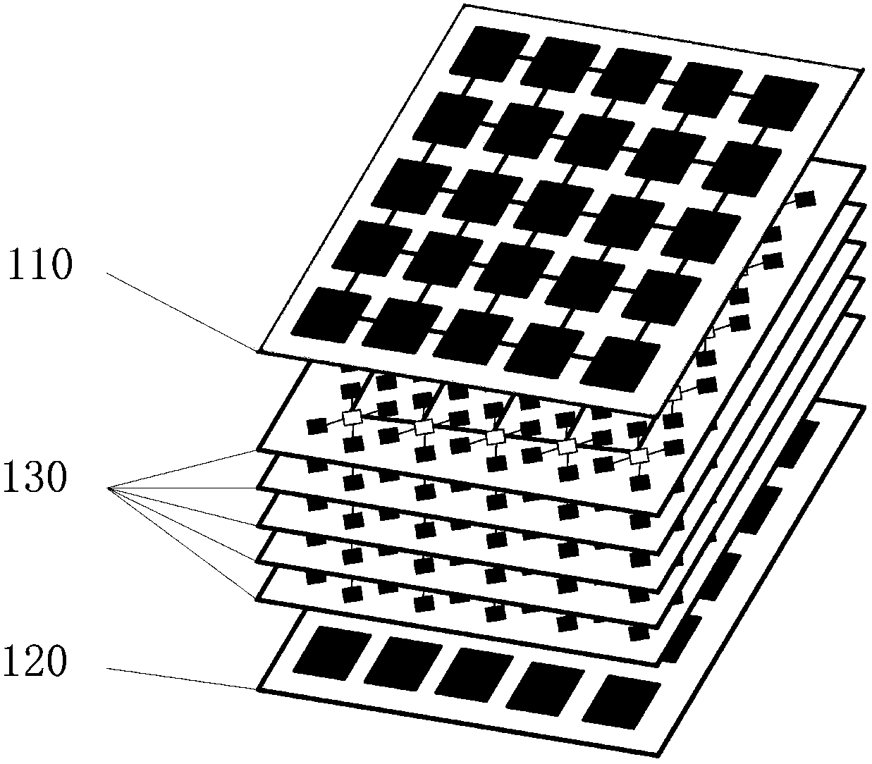
[0025] Aiming at the above technical problems, the present invention carried out innovation and research, and proposed a three-dimensional optical-on-chip network architecture based on stacking faults, see the attached figure 1 , the f...

Embodiment 2

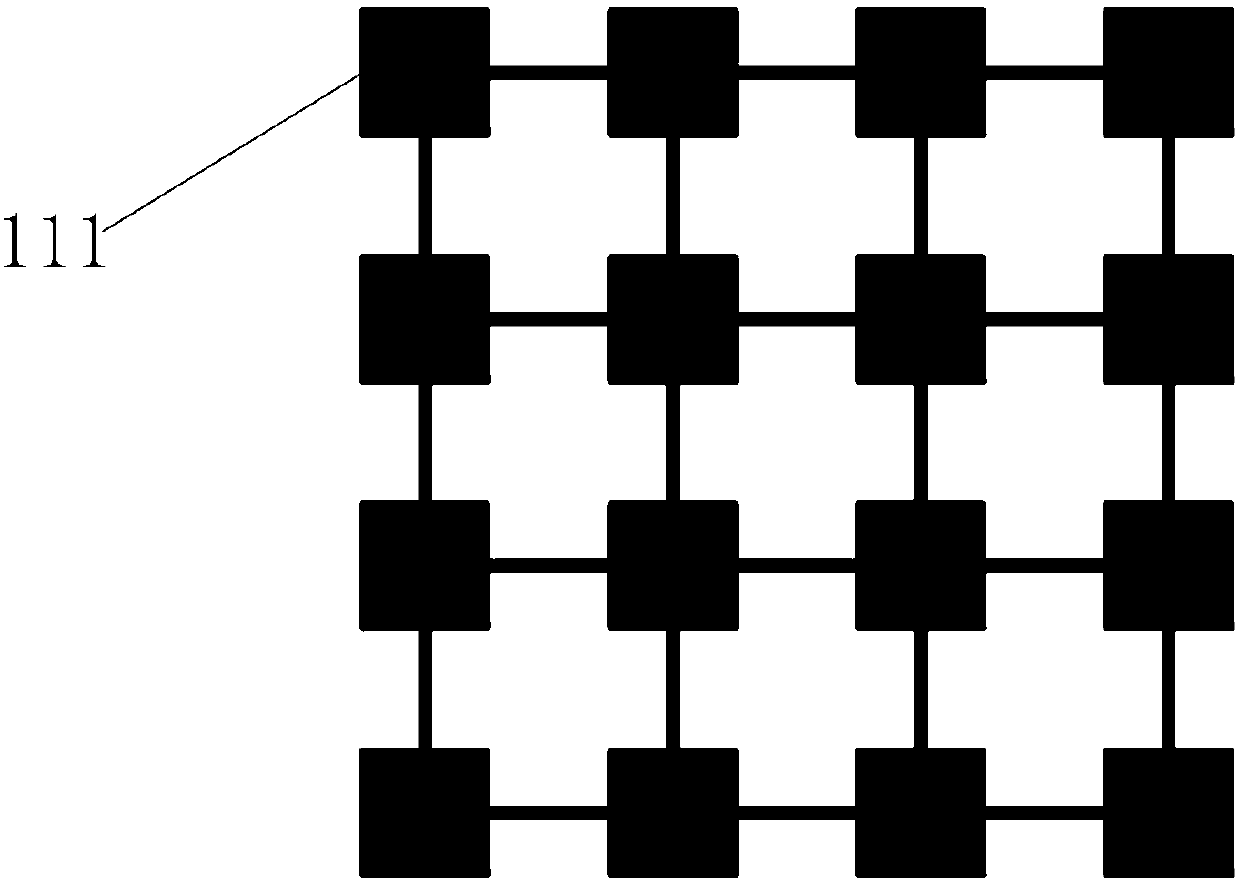
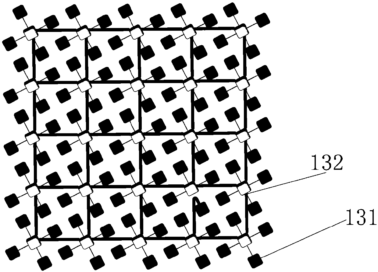
[0028] The fault-based three-dimensional optical on-chip network architecture is the same as that in Embodiment 1. All IP cores and routers in the network use the (x, y, z, m) coordinate system, and the meanings of x, y, and z are the same as the Cartesian three-dimensional coordinate system, where 0 ≤x,y≤(N-1), 0≤z≤6, m is set to 0 for all routers, for the IP core in the middle layer, the positive direction of m is clockwise within the node, 1≤m≤4, And in each intermediate layer, optical / electrical routers at the same position in the optical network and electrical network share the same set of coordinate information, refer to the attached Figure 4 , the coordinate information in each intermediate layer is x=x 0 ,y=y 0 The electrical router 132 in the node is respectively connected to the top layer and the bottom layer through its upper and lower ports and the corresponding two TSVs. The coordinate information is x=x 0 ,y=y 0 The new nine-port optical router 111 and five-p...

Embodiment 3

[0031] The present invention is also a novel nine-port non-blocking optical router, referred to as a nine-port optical router, which is dedicated to a layer-fault-based three-dimensional optical network on chip architecture, which is the same as that of Embodiment 1-2. The new nine-port non-blocking optical router includes nine pairs of full-duplex ports, of which the southbound port, northbound port, westbound port, and eastbound port are respectively used to connect the south, north, west, and east ports of the current nine-port optical router. The nine-port optical router on the side; the remaining five ports of the new nine-port non-blocking optical router: ports z=1, z=2, z=3, z=4, z=5 are respectively used for optical / electrical interface, electrical The / optical interface and TSV connect the electrical routers in the five intermediate layers. Since the network uses the OXY routing algorithm, there is no optical path between the south / north port and the east / west port in ...


PUM


Abstract

The invention provides a fault-based three-dimensional optical on-chip network architecture, a communication method and an optical router, which solve the technical problems of serious blockage in vertical direction, uneven TSV distribution, and big insert loss of a high order optical router in the prior art. The network architecture has seven layers totally, wherein the top layer is an optical network layer and integrated with NXN novel nine-port optical routers; the bottom layer is a pure electric layer and integrated with NXN five-port electric routers; every layer of the middle five layers is integrated with NXNX4 IP cores; the uppermost layer in the middle layers is a reference, and another four layers are staggered along four diagonal line directions respectively to form a fault mechanism; the optical router provides a high-order optical interconnection of the middle layers; the IP internuclear communication includes a node internal part, internal node of layer and interlayer communication; the communication between the inner part of the node and the inside of the layer is carried out through a middle layer optical network; the interlayer communication is realized through a top layer optical network or a bottom layer electric router. The invention solves the problem of serious blockage of vertical direction in a traditional 3D optical on-chip network; the communication between processor cores is high-efficient.

Description

technical field [0001] The invention belongs to the technical field of communication, and relates to a three-dimensional optical on-chip network architecture and communication, in particular to a fault-based three-dimensional optical on-chip network architecture, a communication method and an optical router, which are used for the interconnection and communication of processors in multiprocessor chips. communication. Background technique [0002] The advent of the era of high-performance computing has put forward higher and higher requirements for the performance of processor chips. Future multi-core processors require that the network-on-chip can provide high bandwidth and low latency while reducing network energy consumption as much as possible. However, with the continuous shrinking of the feature size of integrated circuits and the rapid increase of clock frequency, the metal interconnection lines in the traditional electrical interconnection network on chip face many ch...

Claims


Application Information

Patent Timeline
Patent Type & Authority Applications(China)
IPC IPC(8): G06F15/173G06F15/78H04Q11/00
CPCG06F15/17387G06F15/7825H04Q11/0005H04Q11/0062
Inventor 郭雅楠顾华玺杨银堂朱樟明谭伟黄蕾
Owner XIDIAN UNIV
Why Eureka
Try Eureka