Fine pitch package structure

A packaging structure and micro-pitch technology, applied in the direction of electrical components, electrical solid devices, circuits, etc., can solve problems such as inability to cooperate with miniaturized chip conductors

Inactive Publication Date: 2017-10-03
CHIPBOND TECH
View PDF5 Cites 6 Cited by
  • Summary
  • Abstract
  • Description
  • Claims
  • Application Information

AI Technical Summary

Problems solved by technology

[0003] The existing known circuit substrate is used to electrically connect chips, and the circuit substrate has a plurality of circuits, and the circuits are made through patterned metal layers, so the thickness of the metal layer will affect the patterning process. The spacing between adjacent lines, that is to say, when the thickness ...

Method used


Image

  • Fine pitch package structure
  • Fine pitch package structure
  • Fine pitch package structure

Examples


no. 1 example

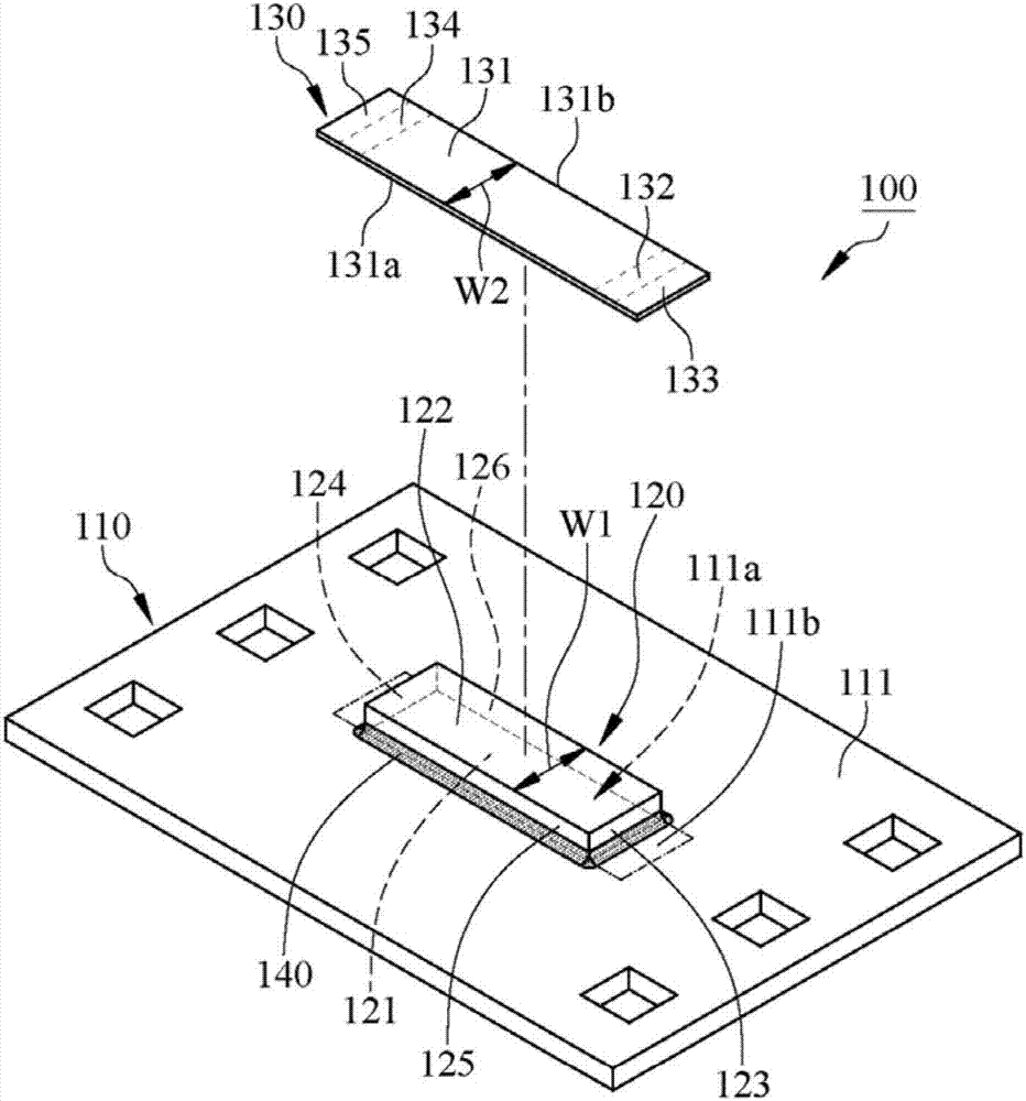
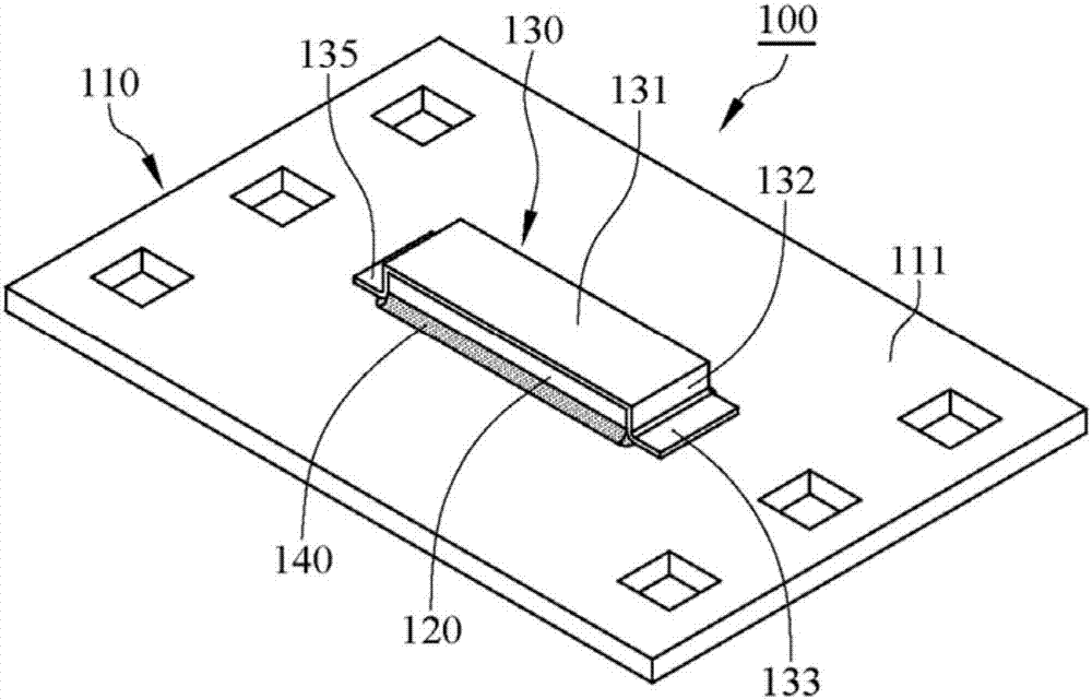
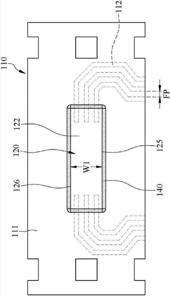
[0049] see figure 1 and figure 2 , which is the first embodiment of the present invention, a micro-pitch packaging structure 100 includes a circuit substrate 110, a chip 120 and a heat sink 130, the chip 120 is located between the circuit substrate 110 and the heat sink 130, the circuit substrate 110 The surface 111 of the surface 111 has a chip setting area 111a and at least one conducting area 111b, the conducting area 111b is located outside the chip setting area 111a, the chip 120 is arranged in the chip setting area 111a and exposes the conducting area 111b, the chip 120 Has a front 121 and a back 122, the front 121 faces the surface 111 of the circuit substrate 110, the flexible heat sink 130 is arranged on the back 122 and the conductive area 111b, the heat sink 130 is used for the chip The heat energy generated by 120 is guided to the air and the circuit substrate 110 to achieve rapid heat dissipation. Preferably, the material of the heat sink 130 can be selected fro...


PUM


Abstract

The invention relates to a fine pitch package structure which includes a line substrate, a chip and a heat dissipating sheet. The line substrate has a plurality of lines. Each line has a thickness of 4-8 [mu]m, and the width among the lines is between 10-18 [mu]m. The chip is disposed on the line substrate, and the right side of the chip faces towards the surface of the line substrate and is in electrical connection to the lines. The heat dissipating sheet is disposed on the back side of the chip and the surface of the line substrate so as to guide the heat generated by the chip to air and the line substrate. The fine pitch package structure can achieve fine effects and the effects of fast heat dissipation by means of the lines and the heat dissipating sheet.

Description

technical field [0001] The present invention relates to a packaging structure, in particular to a packaging structure with fine-pitch circuits. Background technique [0002] In order to meet the needs of miniaturization and high performance of electronic products, the size of the chip is usually miniaturized, and the performance of the chip is improved through IC design to meet the demand, so the conductors in the chip (such as conductor pads or bumps) and The spacing between the conductors must also be miniaturized accordingly. [0003] The existing known circuit substrate is used to electrically connect chips, and the circuit substrate has a plurality of circuits, and the circuits are made through patterned metal layers, so the thickness of the metal layer will affect the patterning process. The spacing between adjacent lines, that is to say, when the thickness of the metal layer is thicker, the spacing between adjacent lines is larger, and when the spacing between adjace...

Claims


Application Information

Patent Timeline
IPC IPC(8): H01L23/31H01L23/367H01L23/48
CPCH01L23/31H01L23/3672H01L23/481H01L2224/16225H01L2224/73204H01L23/3675H01L23/3736H01L23/49816H01L24/04
Inventor 吴非艰谢庆堂徐佑铭吴国玄
Owner CHIPBOND TECH
Why Eureka
Try Eureka