Chip mounter for CSP LEDs, and processing process for chip mounter

A processing technology, LED chip technology, applied in the direction of electrical components, circuits, semiconductor devices, etc., can solve the problems of low yield rate of finished products, difficulty in mass production, general stability and other problems, and achieve high yield rate of finished products and low production cost , The effect of ensuring the stability of the machine

Inactive Publication Date: 2017-10-31
ZHONGSHAN HONGCHANG ELECTRIC & LIGHTING TECH
View PDF5 Cites 14 Cited by
  • Summary
  • Abstract
  • Description
  • Claims
  • Application Information

AI Technical Summary

Problems solved by technology

However, due to the smaller size of unpackaged LEDs compared to traditional chips, and many technical barriers such as higher precision requirements for placement equipment, the current CSP packaged LED placement equipment is difficult to meet the above requirements, and it is difficult to carry out integrated processing and production. Low, often requires multiple equipment to complete the placement process, it is difficult to carry out high-efficiency mass production, high equipment and operating costs, long processing time, low accuracy, general stability, and low yield rate of finished products

Method used


Image

  • Chip mounter for CSP LEDs, and processing process for chip mounter
  • Chip mounter for CSP LEDs, and processing process for chip mounter
  • Chip mounter for CSP LEDs, and processing process for chip mounter

Examples


Embodiment Construction

[0014] It should be understood that the specific embodiments described here are only used to explain the present invention, not to limit the present invention.

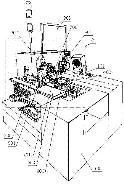
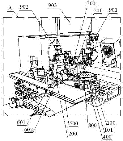
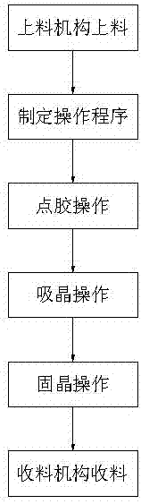
[0015] refer to Figure 1 to Figure 3 , an embodiment of a placement machine for CSP packaged LEDs and its processing technology of the present invention is proposed, the LED chips 101 attached to the blue film 100 arranged in an array can be directly welded and fixed to the substrate 200, and the placement machine includes The frame 300, the crystal suction table 400 which is set on the frame 300 and can be installed with the blue film 100 and makes the blue film 100 tight, and the movable crystal bonding for holding the substrate 200 which is set on the frame 300 Workbench 500 , a dispensing mechanism disposed above the die-bonding workbench 500 and capable of dispensing glue on corresponding pads of the substrate 200 .

[0016] The placement machine also includes a suction crystal with a swing arm 701 that can vac...


PUM


Abstract

The invention discloses a chip mounter for CSP LEDs, and a processing process for the chip mounter. LED chips arranged and attached on a blue film in an array mode can be directly welded and fixed on a substrate; the chip mounter comprises a machine frame, a crystal adsorption table arranged on the machine frame and capable of being equipped with the blue film, a movable crystal fixing worktable arranged on the machine frame and used for bearing the substrate, and an adhesive dispensing mechanism capable of performing adhesive dispensing operation on a corresponding bonding pad of the substrate; the chip mounter further comprises a crystal adsorbing and fixing mechanism with a swing arm capable of performing vacuum adsorption on the LED chips on the blue film on the crystal adsorption table and directly welding and fixing the LED chips to the bonding pad subjected to adhesive dispensing, and an ejector mechanism capable of ejecting the LED chips to facilitate the crystal adsorbing and fixing mechanism to perform adsorption operation on the LED chips; the chip mounter further comprises an image identification control apparatus; the image identification control apparatus consists of an optical crystal adsorption apparatus and an optical crystal fixing apparatus; the chip mounter further comprises an intelligent control apparatus capable of controlling each part of the chip mounter to work; and the chip mounter further comprises a feeding mechanism and a discharging mechanism.

Description

technical field [0001] The invention relates to an LED chip mounter, in particular to a chip mounter for a CSP packaged LED and a processing technique thereof. Background technique [0002] CSP directly covers the phosphor on the chip, which simplifies the production process and reduces the production cost; and there is no support, the thermal resistance is greatly reduced, and the same device volume can provide greater power; moreover, the package is smaller and closer to Point light source, end-user lighting design is more flexible, bringing greater convenience and expanding design breadth to application manufacturers. However, due to the smaller size of unpackaged LEDs compared to traditional chips, and many technical barriers such as higher precision requirements for placement equipment, the current CSP packaged LED placement equipment is difficult to meet the above requirements, and it is difficult to carry out integrated processing and production. Low, often requires ...

Claims


Application Information

Patent Timeline
Patent Type & Authority Applications(China)
IPC IPC(8): H01L33/00H01L33/50H01L33/62
CPCH01L33/50H01L33/62H01L2933/0041H01L2933/0066
Inventor 李杏贤
Owner ZHONGSHAN HONGCHANG ELECTRIC & LIGHTING TECH
Why Eureka
Try Eureka