Defect detection method and device

A defect detection and defect technology, applied in measurement devices, optical testing flaws/defects, image enhancement, etc., can solve the problems of high over-judgment rate, high cost, long debugging cycle, etc., to improve accuracy and reduce over-judgment rate. , The effect of reducing the probability of being judged as a defect

Active Publication Date: 2017-11-07
BOE TECH GRP CO LTD +1
View PDF7 Cites 18 Cited by
  • Summary
  • Abstract
  • Description
  • Claims
  • Application Information

AI Technical Summary

Problems solved by technology

[0003] However, due to defects in the LCD panel, such as Mura (moire phenomenon), the size, area, and shape of the ROI are uncertain, and are easily affected by the environment, especially the light. In the case of a single defect quantization algorithm in the prior art, The quantitative value will not change. Simply changing the detection threshold cannot fundamentally solve the problem of high over-judgment rate caused by defects in the external environment; of course, multi-parameter joint debugging or high-precision cameras can be used method, but the debugging period of this method is long, and changing the model requires re-commissioning, which makes the cost relatively high

Method used


Image

  • Defect detection method and device
  • Defect detection method and device
  • Defect detection method and device

Examples


Embodiment Construction

[0026] The following will clearly and completely describe the technical solutions in the embodiments of the present invention with reference to the accompanying drawings in the embodiments of the present invention. Obviously, the described embodiments are only some, not all, embodiments of the present invention. Based on the embodiments of the present invention, all other embodiments obtained by persons of ordinary skill in the art without making creative efforts belong to the protection scope of the present invention.

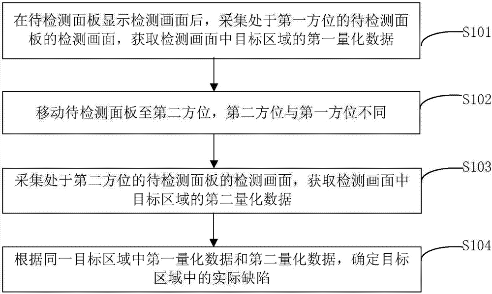
[0027] An embodiment of the present invention provides a defect detection method, for example, an AOI defect detection method, such as figure 1 As shown, the method includes:

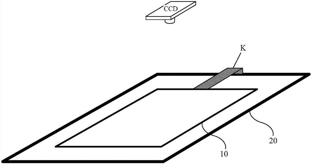
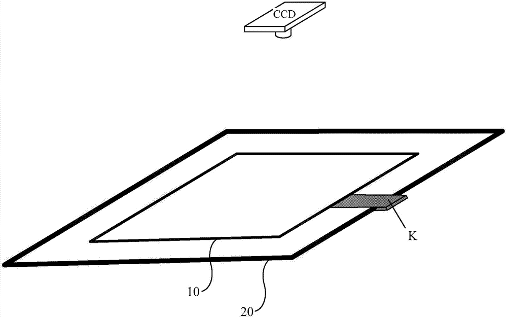
[0028] Step S101 , after the panel to be inspected displays the inspection image, collect the inspection image of the panel to be inspected in the first orientation, and acquire the first quantitative data of the target area in the inspection image.

[0029] Specifically, when the pane...


PUM


Abstract

The embodiment of the invention provides a defect detection method and device, relates to the field of optical automation defect detection, and can lower the excessive judgment rate of a defect through a simple defect detection method. The defect detection method comprises the following steps: after a detection picture is displayed on a panel to be detected, collecting the defection picture of the panel to be detected in a first direction, and obtaining the first quantized data of a target area in the detection picture; moving the panel to be detected to a second direction, wherein the second direct is different from the first direction; collecting the detection picture of the panel to be detected in the second direction, and obtaining the second quantized data of the target area in the detection picture; according to the first quantized data and the second quantized data in the same target area, determining practical defects in the target area.

Description

technical field [0001] The invention relates to the field of optical automatic defect detection, in particular to a defect detection method and device. Background technique [0002] At present, in the factory inspection process of LCD (Liquid Crystal Display, liquid crystal display), the AOI (Automatic Optic Inspection, automatic optical inspection) algorithm process is mostly used to detect the defects of the LCD panel. The algorithm process generally includes ROI (Region of Interest, Target area) segmentation and defect quantification are two key steps. Among them, defect quantification is to quantify the brightness difference of the panel under the lighting screen according to a certain benchmark, and determine the nature of the defect through the comparison of quantitative data and the formulation of relevant defect standards. [0003] However, due to defects in the LCD panel, such as Mura (moire phenomenon), the size, area, and shape of the ROI are uncertain, and are ea...

Claims


Application Information

Patent Timeline
Patent Type & Authority Applications(China)
IPC IPC(8): G01N21/95G01N21/88
CPCG01N21/8851G01N21/95G01N2021/887G01N2021/9513G06T2207/30121G06T7/0004G09G3/006
Inventor 刘泽
Owner BOE TECH GRP CO LTD
Why Eureka
Try Eureka