Semiconductor device

A semiconductor and conductive type technology, applied in the fields of semiconductor devices, semiconductor/solid-state device manufacturing, electrical components, etc., can solve the problems of switching characteristics, increase in charge and discharge time, increase in switching loss, etc., to improve the on-voltage, inhibit the The effect of increased cost

Active Publication Date: 2014-12-17
FUJI ELECTRIC CO LTD
View PDF6 Cites 10 Cited by
  • Summary
  • Abstract
  • Description
  • Claims
  • Application Information

AI Technical Summary

Problems solved by technology

[0015] Therefore, if the capacitance between the gate electrode and the emitter becomes large, there is a problem that the charging and discharging time increases, and not only a problem occurs in switching characteristics, but also a problem in that switching loss increases
In addition, the total loss of the power device is the sum of the steady-state loss determined by the conduction voltage and the switching loss generated during the switching operation.

Method used


Image

  • Semiconductor device
  • Semiconductor device
  • Semiconductor device

Examples


Embodiment approach 1

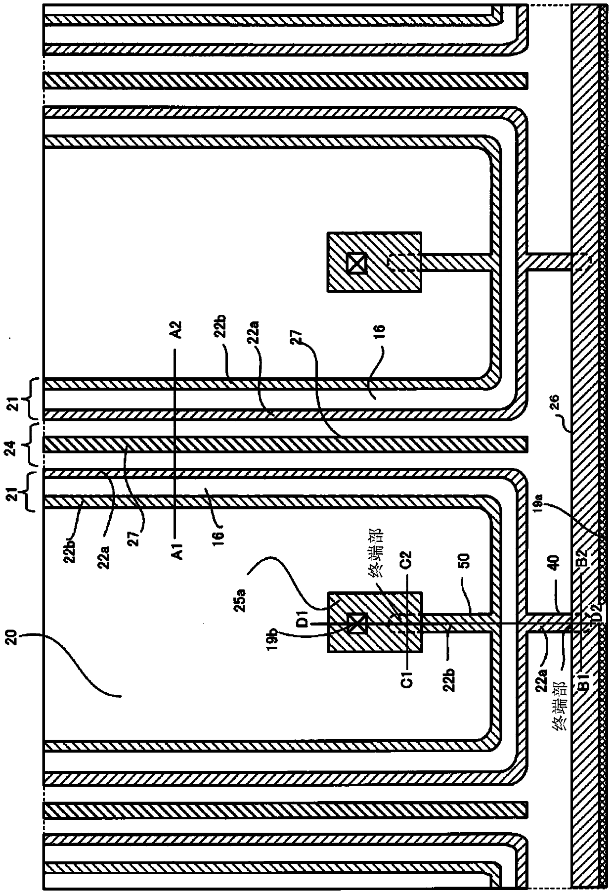
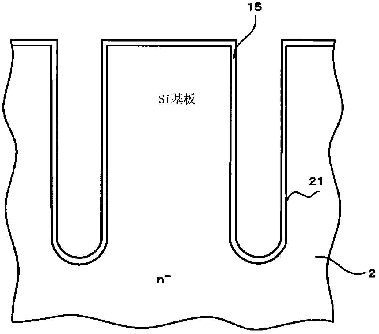
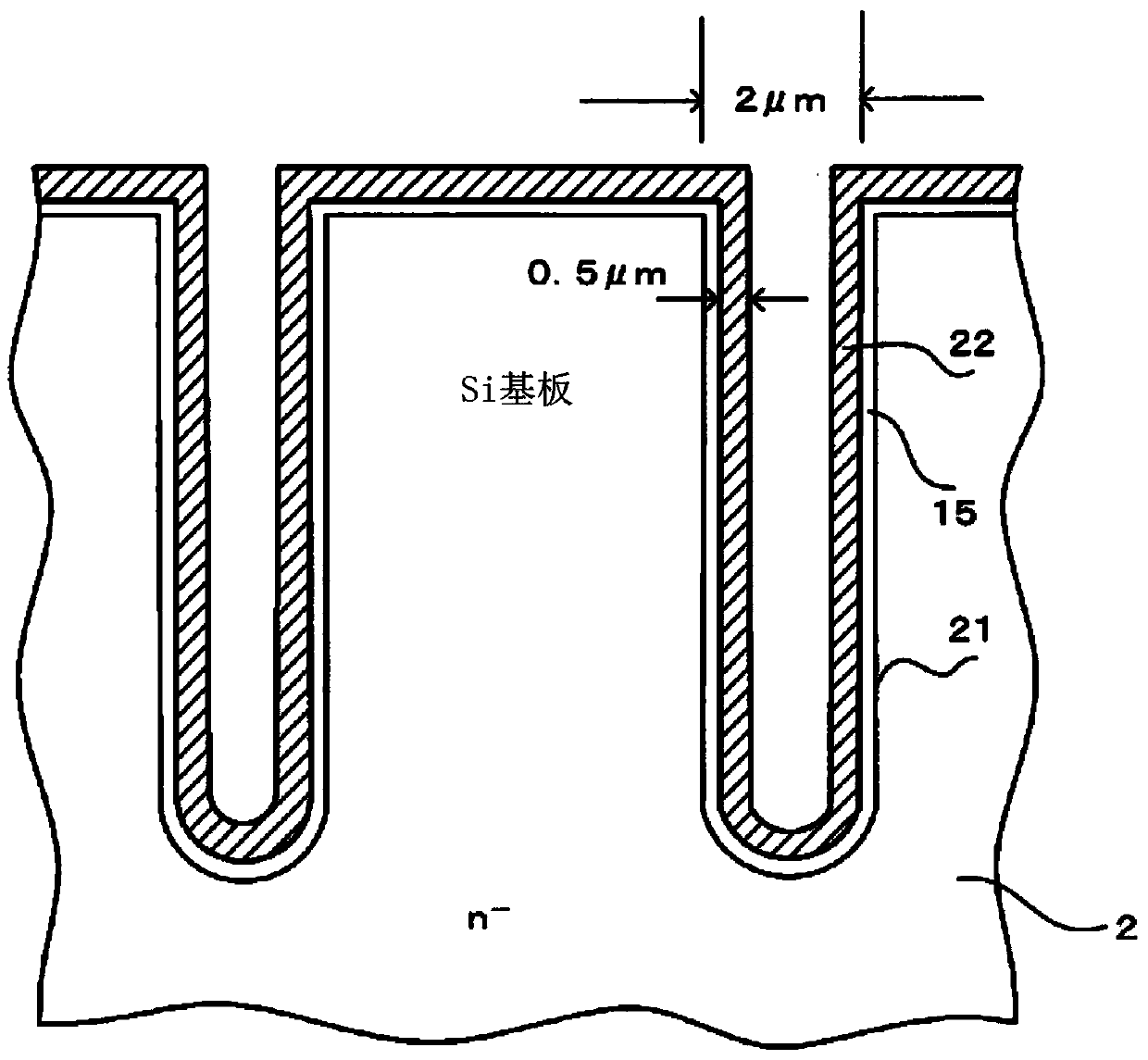
[0087] The configuration of the semiconductor device according to Embodiment 1 will be described. figure 1 It is a plan view showing the planar layout of the main part of the semiconductor device according to the first embodiment. Figure 9 yes means figure 1 A cross-sectional view of the cross-sectional structure at cutting line A1-A2. Figure 10 yes means figure 1 Cross-sectional views of the respective cross-sectional structures at cutting lines B1-B2 and C1-C2. Figure 11 yes means figure 1 A cross-sectional view of the cross-sectional structure at cutting line D1-D2. First, the planar layout of the semiconductor device according to Embodiment 1 will be described. The semiconductor device according to Embodiment 1 includes an active region through which current flows in an on state and a relaxation n - The electric field on the front side of the silicon substrate of the drift layer maintains the withstand voltage region. The voltage-resistant region surrounds th...

Embodiment approach 2

[0124] Next, the configuration of the semiconductor device according to Embodiment 2 will be described. Figure 12 It is a plan view showing the planar layout of the main part of the semiconductor device according to the second embodiment. The semiconductor device according to the second embodiment differs from the semiconductor device according to the first embodiment in the planar shapes of the second trench 40 and the third trench 50 . Specifically, as Figure 12 As shown, the second trench 40 has a substantially U-shaped planar shape, and both ends thereof are connected to the outer sidewalls of the first trench 21 . That is, a substantially rectangular annular planar shape is formed by the second groove 40 and a part of the first groove 21 . The second groove 40 may be formed so that both ends thereof are connected to the outer side walls of the first groove 21 and form a substantially rectangular annular planar shape together with the first groove 21, and is not limite...

Embodiment approach 3

[0131] Figure 14 It is a plan view showing the planar layout of the main part of the semiconductor device according to the third embodiment. The semiconductor device of Embodiment 3 differs from the semiconductor device of Embodiment 1 in the number of second trenches 40 relative to one third trench 50 and the positions where the second trenches 40 are arranged. Specifically, in Embodiment 1, the second groove 40 and the third groove 50 are arranged to face each other with the first groove 21 interposed therebetween. More specifically, the second groove 40 and the third groove 50 are arranged on the same straight line crossing the first groove 21 . In contrast, in Embodiment 3, as Figure 14 As shown, two second grooves 40 are arranged relative to one third groove 50 , and the second groove 40 and the third groove 50 are alternately arranged with the first groove 21 placed in the middle. More specifically, for example, a plurality of second trenches 40 are provided with re...


PUM


Abstract

This semiconductor device is characterized in being provided with: a first gate electrode (22a), which is provided on the inner side of a first insulating film, said first gate electrode being provided along one side wall of a first trench (21), and which is provided inside of a second trench (40); a shield electrode (22b), which is provided on the inner side of a second insulating film, said shield electrode being provided along the other side wall of the first trench (21), and which is provided inside of a third trench (50); a gate runner, which has a part thereof provided on the first gate electrode (22a) by having the second trench (40) extended, and which is connected to the first gate electrode (22a); and an emitter polysilicon layer (25a), which has a part thereof provided on the shield electrode (22b) by having the third trench (50) extended, and which is connected to the shield electrode (22b). Consequently, turn-on characteristics are improved with an increase of a small number of process steps, while suppressing cost increase and deterioration of yield rate.

Description

technical field [0001] The present invention relates to semiconductor devices, and more particularly to trench-gate insulated-gate bipolar transistors (IGBTs). Background technique [0002] In the course of promoting the reduction in power consumption of power conversion devices, there are great expectations for reduction in power consumption of power devices that play a central role in the power conversion devices. In this power device, low on-voltage can also be achieved by the conductance modulation effect, and the use of insulated gate bipolar transistors (IGBT: Insulated Gate Bipolar Transistor), which can be easily controlled by voltage-driven gate control, has become increasingly popular. more stable. [0003] As the MOS gate (insulated gate composed of metal-oxide film-semiconductor) structure of this IGBT, there are known planar gate type IGBTs with a gate electrode along the wafer surface and a striped planar pattern on the wafer surface. A trench gate type IGBT ...

Claims


Application Information

Patent Timeline
Patent Type & Authority Applications(China)
IPC IPC(8): H01L29/78H01L21/336H01L29/739
CPCH01L29/4236H01L29/4238H01L29/66348H01L29/7397H01L29/407H01L29/7811H01L29/7813H01L29/0619H01L29/1095H01L29/41708H01L29/42304H01L29/4916
Inventor 小野泽勇一高桥英纪吉村尚
Owner FUJI ELECTRIC CO LTD
Why Eureka
Try Eureka