Liquid crystal panel dark spot repair method and array substrate structure

An array substrate structure and liquid crystal panel technology, applied in the fields of optics, instruments, electrical components, etc., can solve problems such as low success rate, failure to connect pixel electrodes 100 and common electrode lines 400 on the array substrate side, repair failure, etc., and achieve easy operation , Improve the success rate of repair and simplify the process

Active Publication Date: 2017-11-07
SHENZHEN CHINA STAR OPTOELECTRONICS TECH CO LTD
View PDF12 Cites 19 Cited by
  • Summary
  • Abstract
  • Description
  • Claims
  • Application Information

AI Technical Summary

Problems solved by technology

The success rate of this traditional repair method is low, especially for COA (Color Filter On Array) products where the color filter is arranged on the side of the array substrate. The distance between the common electrode lines 400 is relatively large, and it is easy to cause the connection failure between the pixel electrode 100 and the common electrode lines 400 on the array substrate side due to the interference of the color resist layer, thus resulting in repair failure

Method used


Image

  • Liquid crystal panel dark spot repair method and array substrate structure
  • Liquid crystal panel dark spot repair method and array substrate structure
  • Liquid crystal panel dark spot repair method and array substrate structure

Examples


Embodiment Construction

[0032] In order to further illustrate the technical means adopted by the present invention and its effects, the following describes in detail in conjunction with preferred embodiments of the present invention and accompanying drawings.

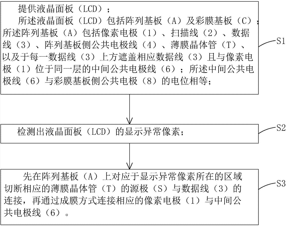
[0033] see figure 2 , the present invention firstly provides a method for repairing dark spots of a liquid crystal panel, comprising the following steps:

[0034] Step S1, providing a liquid crystal panel LCD.

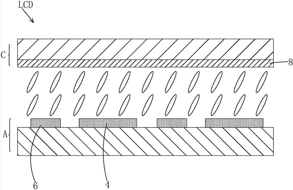
[0035] The liquid crystal panel such as image 3 As shown, it includes an array substrate A and a color filter substrate C.

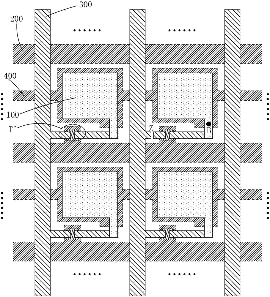
[0036] Such as Figure 4 As shown, the array substrate A includes a plurality of pixel electrodes 1 arranged in an array, a plurality of scanning lines 2 extending in the lateral direction corresponding to each row of pixel electrodes 1 , and a plurality of scanning lines 2 extending in the longitudinal direction corresponding to each column of pixel electrodes 1 . A plurality of data lines 3, a plurality o...


PUM


Abstract

The invention provides a liquid crystal panel dark spot repair method and an array substrate structure. The liquid crystal panel dark spot repair method comprises the steps that after a display abnormal pixel of a liquid crystal panel is detected, connection of a data line and a source electrode of a corresponding thin film transistor is cut off on the region, corresponding to the display abnormal pixel, of an array substrate, a corresponding pixel electrode and a middle common electrode wire are connected in a film forming mode, due to the fact that the middle common electrode wire is equal to the common electrode on the color film substrate side in potential, the voltage difference between the array substrate of the liquid crystal panel and the region, where the display abnormal pixel is located, of the color film substrate is 0, and the abnormal pixel is in the dark state; due to the fact that the pixel electrode and the middle common electrode wire are located on the same layer, the middle common electrode wire and the corresponding pixel electrode are connected in the film forming mode to achieve dark spot repair, compared with an existing punching repairing mode, working procedures are simplified, no disturbance caused by a color resistance layer in a COA type liquid crystal panel is avoided, and the display abnormal pixel repair success rate can be increased.

Description

technical field [0001] The invention relates to the field of display technology, in particular to a liquid crystal panel dark spot repair method and an array substrate structure. Background technique [0002] Thin Film Transistor Liquid Crystal Display (TFT-LCD) is widely used in televisions, mobile phones, computers and other fields due to its advantages of large size, high integration, powerful functions, flexible process, and low cost. Mainstream display. [0003] Liquid crystal display panel, referred to as liquid crystal panel, is the main part of TFT-LCD. It usually consists of a color filter substrate (ColorFilter, CF), a thin film transistor array substrate (Thin Film Transistor Array Substrate, TFTArray Substrate) and a filling on the two substrates. The working principle is to control the rotation of the liquid crystal molecules in the liquid crystal layer by applying a driving voltage on the two glass substrates, and refract the light from the backlight module to...

Claims


Application Information

Patent Timeline
Patent Type & Authority Applications(China)
IPC IPC(8): G02F1/13G02F1/1362G02F1/1368H01L27/12H01L21/77
CPCG02F1/1309G02F1/136259G02F1/136286G02F1/1368G02F1/136263H01L27/1244H01L27/1296
Inventor 刘娜徐向阳
Owner SHENZHEN CHINA STAR OPTOELECTRONICS TECH CO LTD
Why Eureka
Try Eureka