Shifting register, driving method, grid driving circuit and display device

A shift register and driving signal technology, applied in static memory, digital memory information, instruments, etc., can solve the problems of flickering display screen, large jump voltage ΔVp, afterimage, etc.

Active Publication Date: 2017-11-10
BOE TECH GRP CO LTD +1
View PDF12 Cites 7 Cited by
  • Summary
  • Abstract
  • Description
  • Claims
  • Application Information

AI Technical Summary

Problems solved by technology

However, the existing gate drive circuit cannot easily output a scan signal with a chamfered waveform, so that when the display transistor is turned on to off, due to the large coupling capacitance between the gate and the drain of the display transistor, The jump voltage ΔVp generated by the voltage on the pixel electrode is relatively large, resulting in problems such as flickering and afterimages when the display panel displays images.

Method used


Image

  • Shifting register, driving method, grid driving circuit and display device
  • Shifting register, driving method, grid driving circuit and display device
  • Shifting register, driving method, grid driving circuit and display device

Examples


Embodiment 1

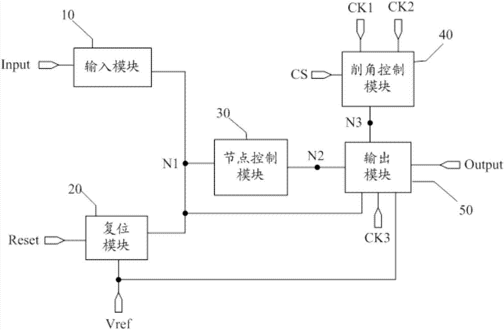
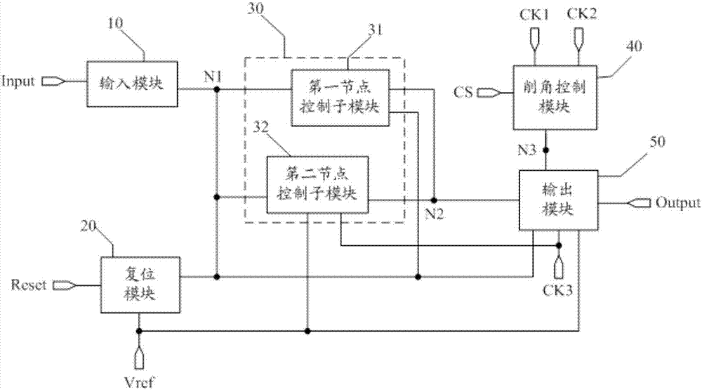
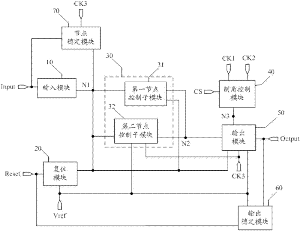
[0129] by Figure 4 The structure of the shift register shown is taken as an example to describe its working process, wherein the signal of the reference voltage signal terminal Vref is a low potential signal, and the corresponding input and output timing diagram is as follows Figure 5 shown. Specifically, choose the Figure 5 In the shown input and output timing diagram, there are five stages: input stage T1, input holding stage T2, output stage T3, output chamfering stage T4 and reset stage T5. Wherein, Va represents the amplitude of the signal of the first clock signal terminal CK1, Vb represents the amplitude of the third clock signal terminal CK3, and Vc represents the amplitude of the signal of the third node N3 in the output chamfering phase T4; wherein, Va >Vb.

[0130] In the input phase T1, Input=1, Reset=0, CK1=0, CK2=0, CK3=1, CS=0.

[0131] Since Input=1, the eleventh switch transistor M11 is turned on to provide the high potential signal of the input signal ...


PUM


Abstract

The invention discloses a shifting register, a driving method, a grid driving circuit and a display device. The shifting register comprises an input module, a return module, a node control module, a cutting angle control module and an output module. Due to adoption of the cutting angel control module and with cooperation of the five modules, the amplitude of a scanning signal output from a driving signal output end can be changed to form a scanning signal with a cutting angle waveform, and when the scanning signal with the cutting angle waveform is input into different pixel units of corresponding rows through different rows of grid lines in sequence, the leaping voltage delta Vp can be reduced, so that phenomena such as flicker and residual images of a display panel can be reduced, and the display quality of the display panel is improved.

Description

technical field [0001] The invention relates to the field of display technology, in particular to a shift register, a driving method thereof, a gate driving circuit and a display device. Background technique [0002] With the rapid development of display technology, the display panel is more and more developed towards the direction of high integration and low cost. Among them, the gate driver on array (Gate Driver on Array, GOA) technology integrates the thin film transistor (Thin Film Transistor, TFT) gate switching circuit on the array substrate of the display panel to form a scan drive for the display panel, so that the gate driver can be omitted. The wiring space of the Bonding area of ​​the integrated circuit (Integrated Circuit, IC) and the fan-out (Fan-out) area can not only reduce the product cost in terms of material cost and manufacturing process, but also enable the display panel to achieve Beautiful design with symmetry on both sides and narrow borders; moreover...

Claims


Application Information

Patent Timeline
Patent Type & Authority Applications(China)
IPC IPC(8): G09G3/20G09G3/36G11C19/28
CPCG09G3/20G09G3/36G11C19/28G09G2320/0257G09G2310/0286G09G2320/0247G09G3/3677G09G2320/0219G09G2330/02G09G2310/06G09G2310/08
Inventor 赵剑李环宇司秀丽
Owner BOE TECH GRP CO LTD
Why Eureka
Try Eureka