Supercharge Your Innovation With Domain-Expert AI Agents!

A light emitting diode and its manufacturing method

A technology for light-emitting diodes and a manufacturing method, which is applied to semiconductor devices, electrical components, circuits, etc., can solve the problems of reduced crystal integrity of the MQW layer, affecting crystal quality and luminous brightness, etc., and achieves the effect of improving LED luminous efficiency and reducing voltage.

Active Publication Date: 2019-06-11
HC SEMITEK SUZHOU
View PDF5 Cites 0 Cited by
  • Summary
  • Abstract
  • Description
  • Claims
  • Application Information

AI Technical Summary

Problems solved by technology

[0006] In order to solve the problem that excessive doping of Si element in the quantum barrier layer in the prior art will reduce the crystalline integrity of the MQW layer and affect the crystal quality and luminous brightness, too little Si element doping in the quantum barrier layer will not be effective. There are problems of reducing the voltage and improving the quality of the crystal, the embodiment of the present invention provides a light emitting diode and its manufacturing method

Method used


Image

  • A light emitting diode and its manufacturing method
  • A light emitting diode and its manufacturing method

Examples


Embodiment 1

[0028] An embodiment of the present invention provides a light emitting diode, figure 1 It is a schematic structural diagram of a light emitting diode provided by an embodiment of the present invention, such as figure 1 As shown, the light-emitting diode includes a substrate 1, and a low-temperature buffer layer 2, a high-temperature buffer layer 3, an N-type layer 4, an MQW layer 5, an electron blocking layer 6, a P-type layer 7, and an activation layer sequentially stacked on the substrate 1. Contact the P-type layer 8 .

[0029] Among them, the MQW layer 5 includes a first sublayer 51, a second sublayer 52, and a third sublayer 53 grown in sequence, and each sublayer is a laminated structure in which quantum well layers and quantum barrier layers are grown alternately, and the quantum barrier layer is doped with There is Si element, the doping concentration of Si in the quantum barrier layer in the third sublayer 53 is greater than the doping concentration of Si in the qua...

Embodiment 2

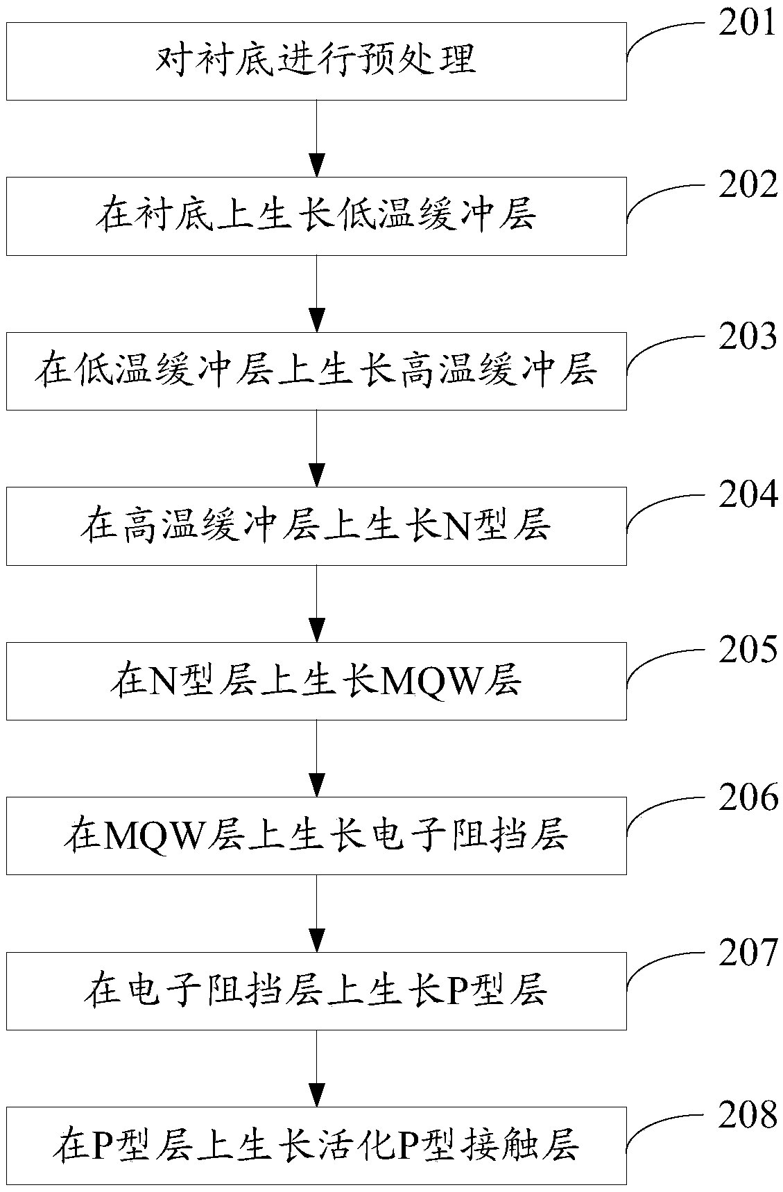
[0046] An embodiment of the present invention provides a method for manufacturing a light-emitting diode, which is suitable for manufacturing the light-emitting diode provided in Embodiment 1. figure 2 It is a flowchart of a method for preparing a light-emitting diode provided by an embodiment of the present invention, such as figure 2 As shown, the manufacturing method includes:

[0047] Step 201, performing pretreatment on the substrate.

[0048] Optionally, the substrate is sapphire with a thickness of 630-650um.

[0049] In this embodiment, Veeco K465i or C4MOCVD (Metal Organic Chemical VaporDeposition, metal organic compound chemical vapor deposition) equipment is used to realize the LED growth method. Using high-purity H 2 (hydrogen) or high-purity N 2 (nitrogen) or high purity H 2 and high purity N 2 The mixed gas as the carrier gas, high-purity NH 3 As the N source, trimethylgallium (TMGa) and triethylgallium (TEGa) are used as the gallium source, trimethylind...


PUM


Abstract

The invention discloses a light-emitting diode and a manufacturing method therefor, and belongs to the technical field of semiconductors. An MQW layer of the light-emitting diode consists of three sublayers, and the three sublayers comprise a first sublayer, a second sublayer and a third sublayer, wherein the first, second and third sublayers grow sequentially. Each sublayer is a laminated structure where a quantum well layer and a quantum barrier layer grow alternately. Each quantum barrier layer is doped with Si elements, and the doping concentration of Si in the quantum barrier layer of the third sublayer is greater than the doping concentration of Si in the quantum barrier layer of the first sublayer. The doping concentration of Si in the quantum barrier layer of the first sublayer is greater than the doping concentration of Si in the quantum barrier layer of the second sublayer. According to the invention, the doping concentration of Si in the second sublayer is set to be the minimum, so as to forma concave doping mode. The second sublayer serves as a temporary storage region of electrons, and better current expanding can be formed between the second sublayer and the first and third sublayers, thereby effectively reducing the voltage, and improving the luminous efficiency of the LED.

Description

technical field [0001] The invention relates to the technical field of semiconductors, in particular to a light emitting diode and a manufacturing method thereof. Background technique [0002] LED (Light Emitting Diode, Light Emitting Diode) is a semiconductor electronic component that can emit light. As an efficient, environmentally friendly and green new solid-state lighting source, it is being rapidly and widely used, such as traffic lights, car interior and exterior lights, urban landscape lighting, mobile phone backlight, etc. Improving the luminous efficiency of chips is the goal that LEDs are constantly pursuing. [0003] Existing LEDs include a substrate and an epitaxial layer stacked on the substrate. The epitaxial layer includes a low-temperature buffer layer, a high-temperature buffer layer, an N-type layer, an MQW (Multiple Quantum Well, multiple quantum well) layer, Electron blocking layer and P-type layer. Among them, the MQW is cyclically grown by the quantu...

Claims


Application Information

Patent Timeline
Patent Type & Authority Patents(China)
IPC IPC(8): H01L33/06H01L33/32H01L33/00
CPCH01L33/007H01L33/06H01L33/325
Inventor 姚振从颖胡加辉李鹏
Owner HC SEMITEK SUZHOU
Features
  • R&D
  • Intellectual Property
  • Life Sciences
  • Materials
  • Tech Scout
  • Unparalleled Data Quality
  • Higher Quality Content
  • 60% Fewer Hallucinations
Learn More