
Silicon carbide device packaging structure and manufacturing method based on three-layer dbc substrate

A technology of device packaging and silicon carbide, which is applied in semiconductor/solid-state device manufacturing, semiconductor devices, electric solid-state devices, etc., can solve problems such as increasing package size and additional resistance, limiting package heat dissipation capacity, and reducing package reliability, etc., to achieve shortening The effect of interconnection distance, increased heat dissipation path, and increased reliability

Active Publication Date: 2019-06-25
INST OF ELECTRONICS ENG CHINA ACAD OF ENG PHYSICS
View PDF5 Cites 0 Cited by
  • Summary
  • Abstract
  • Description
  • Claims
  • Application Information

AI Technical Summary

Problems solved by technology

For the packaging of high-temperature devices, due to the limitation of packaging technology and the flexibility of packaging materials, most of them use wire bonding to realize the interconnection of electrodes and substrates, which not only increases the package size and additional resistance, but also reduces the reliability of the package. The development of power devices will also gradually pay attention to the heat dissipation of the package. The current heat dissipation in a single direction limits the further increase of the package temperature. Most modules now use a direct copper-clad substrate as the base, and realize interconnection through wire bonding and external terminals. Although the heat dissipation path is increased to a certain extent and the reliability is improved, the existence of leads will inevitably bring about large additional inductance and resistance, and the heat dissipation on one side also limits the further improvement of the heat dissipation capability of the package, and the large parasitic parameters And too high chip junction temperature will bring a series of reliability problems, so it is necessary to optimize the packaging structure and packaging method

Method used


Image

  • Silicon carbide device packaging structure and manufacturing method based on three-layer dbc substrate
  • Silicon carbide device packaging structure and manufacturing method based on three-layer dbc substrate
  • Silicon carbide device packaging structure and manufacturing method based on three-layer dbc substrate

Examples


Embodiment Construction

[0036] The technical solutions in the embodiments of the present invention will be clearly and completely described below in conjunction with the drawings in the embodiments of the present invention. Obviously, the described embodiments are only part of the embodiments of the present invention, not all of them. Based on the embodiments of the present invention, all other embodiments obtained by persons of ordinary skill in the art without making creative efforts belong to the protection scope of the present invention.

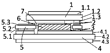
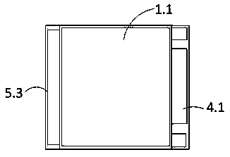
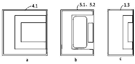
[0037] The embodiment of the present invention provides a packaging structure and manufacturing method of a silicon carbide power device based on a three-layer DBC substrate, such as figure 1 As shown, the package includes: three-layer patterned DBC substrates 1, 4, 5, vertical silicon carbide power devices 6 packaged between the three-layer DBC substrates, nano-silver solder paste 2 and 3, and high-temperature-resistant filler 7; the package shell , and extern...


PUM

PropertyMeasurementUnit
thermal resistanceaaaaaaaaaa
strengthaaaaaaaaaa

Abstract

The invention discloses a three-layer DBC substrate-based silicon carbide package structure and a manufacturing method thereof. The package structure comprises an upper structure, an intermediate structure, a lower structure, two layers of nanometer silver welding paste, a longitudinal silicon carbide power chip and a high-temperature resistant filler, wherein the upper structure, the intermediate structure and the lower structure are formed by a three-layer pattern DBC substrate, a chip electrode is led out without a lead by patterning of the DBC substrate and connection by the nanometer silver welding paste, the interconnection area is expanded, the connection distance is shorted, and the additional resistance and inductance are reduced; moreover, leading-out electrodes are arranged on different planes, and the insulation performance is not affected by the thickness of an intermediate layer due to the design of a DBC pattern; meanwhile, the intermediate layer of the package structure is used as a heat dissipation passage, heat of upper-layer DBC can be transferred to lower-layer DBC, the heat dissipation passages are added, and heat generated by the chip also can be dissipated by an upper surface and a lower surface under the condition that a heat dissipation plate is not additionally arranged; and compared with other package modes, the package structure is simple in structure, enough in raw material and high in maneuverability, and has relatively universal applicability.

Description

technical field [0001] The invention relates to the field of semiconductor power device packaging, in particular to a silicon carbide device packaging structure and manufacturing method based on a three-layer DBC substrate. Background technique [0002] With the continuous development of the electronics industry, the performance requirements of electronic devices are constantly increasing, and the improvement of device power and device power density has become an inevitable trend. With the continuous research of the third-generation semiconductor materials in the field of semiconductor devices, the ensuing convenience It is the packaging problem of power devices. For silicon carbide devices, due to the superiority of the silicon carbide material itself, it has the advantages of high breakdown electric field strength, good thermal stability and high carrier saturation drift speed. The corresponding devices have high temperature resistance, and their maximum operating temperat...

Claims


Application Information

Patent Timeline
Patent Type & Authority Patents(China)
IPC IPC(8): H01L23/31H01L23/367H01L23/48H01L21/56H01L29/861
CPCH01L21/56H01L23/3114H01L23/3121H01L23/367H01L23/48H01L29/861H01L2224/33
Inventor 杨英坤李俊焘代刚张龙肖承全张林徐星亮向安周阳古云飞崔潆心银杉李志强
Owner INST OF ELECTRONICS ENG CHINA ACAD OF ENG PHYSICS
Learn More