Fan-out type package structure and preparation method thereof

A packaging structure, fan-out technology, used in semiconductor/solid-state device manufacturing, electrical components, electrical solid-state devices, etc., can solve the problem that the semiconductor chip is prone to shaking, affects the performance of the package structure, and the semiconductor chip has poor contact with the rewiring layer, etc. problem, to achieve the effect of increased adhesion, good contact, and guaranteed performance

Inactive Publication Date: 2017-11-24
SJ SEMICON JIANGYIN CORP
View PDF4 Cites 5 Cited by
  • Summary
  • Abstract
  • Description
  • Claims
  • Application Information

AI Technical Summary

Problems solved by technology

[0004] In view of the above-mentioned shortcomings of the prior art, the purpose of the present invention is to provide a fan-out packaging structure and its preparation method, which is used to solve the problem that the semiconductor

Method used


Image

  • Fan-out type package structure and preparation method thereof
  • Fan-out type package structure and preparation method thereof
  • Fan-out type package structure and preparation method thereof

Examples


Embodiment 1

[0060] see figure 1 , this embodiment provides a method for preparing a fan-out packaging structure, the method for preparing a fan-out packaging structure includes the following steps:

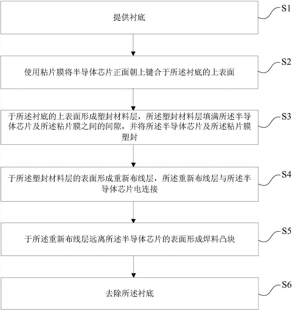
[0061] 1) Provide the substrate;

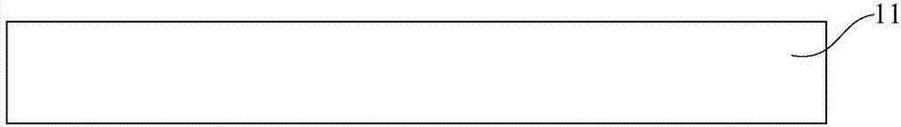
[0062] 2) Bonding the semiconductor chip face up to the upper surface of the substrate using an adhesive film;

[0063] 3) forming a plastic sealing material layer on the upper surface of the substrate, the plastic sealing material layer fills the gap between the semiconductor chip and the adhesive film, and plastic seals the semiconductor chip and the adhesive film ;

[0064] 4) forming a rewiring layer on the surface of the plastic packaging material layer, the rewiring layer is electrically connected to the semiconductor chip;

[0065] 5) forming solder bumps on the surface of the rewiring layer away from the semiconductor chip;

[0066] 6) The substrate is removed.

[0067] In step 1), see figure 1 Step S1 in and figure 2 , providing a substrate 11...

Embodiment 2

[0107] read on Figure 9 , this embodiment also provides a fan-out packaging structure, the fan-out packaging structure is prepared by the preparation method described in the first embodiment, the fan-out packaging structure includes: a rewiring layer 16, the The rewiring layer 16 includes opposite first surfaces and second surfaces; a semiconductor chip 13, the semiconductor chip 13 is located on the first surface of the rewiring layer 16, and the front side of the semiconductor chip 13 is connected to the rewiring layer. The layer 16 is electrically connected; the adhesive film 14, the adhesive film 14 is located on the back side of the semiconductor chip 13; the molding material layer 15, the molding material layer 15 is located on the first surface of the rewiring layer 16, the The plastic sealing material layer 15 fills up the gap between the semiconductor chip 13 and the adhesive film 14, and plastics the semiconductor chip 13 and the adhesive film 14; solder bumps 17, t...


PUM


Abstract

The invention provides a fan-out type package structure and a preparation method thereof. The fan-out type package structure comprises a rewiring layer, a semiconductor chip arranged on a first surface of the rewiring layer, a die-attach film arranged on the back surface of the semiconductor chip, a plastic package material layer arranged on the first surface of the rewiring layer, and a solder bump arranged on a second surface of the rewiring layer. According to the fan-out type package structure, the back surface of the semiconductor chip is provided with the die-attach film, and in the preparation process, the semiconductor chip is mounted on the upper surface of a substrate with the right face up through the die-attach film, so that the binding force between the semiconductor chip and the substrate is increased greatly, and the semiconductor chip can be firmly attached onto the upper surface of the substrate; and it is ensured that the semiconductor chip does not shift in the follow-up preparation processes of plastic package and the like, the semiconductor chip and the rewiring layer are in good contact, and thus performance of the fan-out type package structure can be ensured.

Description

technical field [0001] The invention relates to the technical field of semiconductor packaging, in particular to a fan-out packaging structure and a preparation method thereof. Background technique [0002] Lower cost, more reliable, faster and higher density circuits are the goals pursued by integrated circuit packaging. In the future, integrated circuit packaging will increase the integration density of various electronic components by continuously reducing the minimum feature size. Currently, advanced packaging methods include: Wafer Level Chip Scale Packaging (WLCSP), Fan-Out Wafer Level Package (FOWLP), Flip Chip, Package on Package (Package on Package, POP) and so on. [0003] Fan-out wafer-level packaging is an embedded chip packaging method for wafer-level processing. It is currently one of the advanced packaging methods with more input / output ports (I / O) and better integration flexibility. Compared with conventional wafer-level packaging, fan-out wafer-level pack...

Claims


Application Information

Patent Timeline
IPC IPC(8): H01L23/31H01L23/48H01L23/488H01L21/56H01L21/60H01L23/29
CPCH01L21/563H01L21/568H01L23/293H01L23/3114H01L23/3121H01L24/11H01L2224/02331H01L2224/02379H01L2224/02381H01L2224/11
Inventor 陈彦亨林正忠
Owner SJ SEMICON JIANGYIN CORP
Why Eureka
Try Eureka