Organic light emitting diode display panel and manufacturing method thereof

A technology for light-emitting diodes and display panels, which is applied in the manufacturing of semiconductor/solid-state devices, semiconductor devices, electrical components, etc., can solve problems such as affecting the display effect of organic light-emitting diode display panels and uneven thickness of the organic light-emitting functional layer 3

Active Publication Date: 2020-08-11
BOE TECH GRP CO LTD
View PDF10 Cites 0 Cited by
  • Summary
  • Abstract
  • Description
  • Claims
  • Application Information

AI Technical Summary

Problems solved by technology

[0004] However, during the drying process, the ink sprayed into the opening 21 will climb along the pixel defining layer 2 around the opening 21, forming an organic light-emitting functional layer 3 with thick edges and thin middle, that is, the formed organic light-emitting layer 3 The thickness of the functional layer 3 is uneven, thus affecting the display effect of the OLED display panel

Method used


Image

  • Organic light emitting diode display panel and manufacturing method thereof
  • Organic light emitting diode display panel and manufacturing method thereof
  • Organic light emitting diode display panel and manufacturing method thereof

Examples


Embodiment Construction

[0046] The following will clearly and completely describe the technical solutions in the embodiments of the present invention with reference to the accompanying drawings in the embodiments of the present invention. Obviously, the described embodiments are some of the embodiments of the present invention, but not all of them. Based on the embodiments of the present invention, all other embodiments obtained by persons of ordinary skill in the art without making creative efforts belong to the protection scope of the present invention.

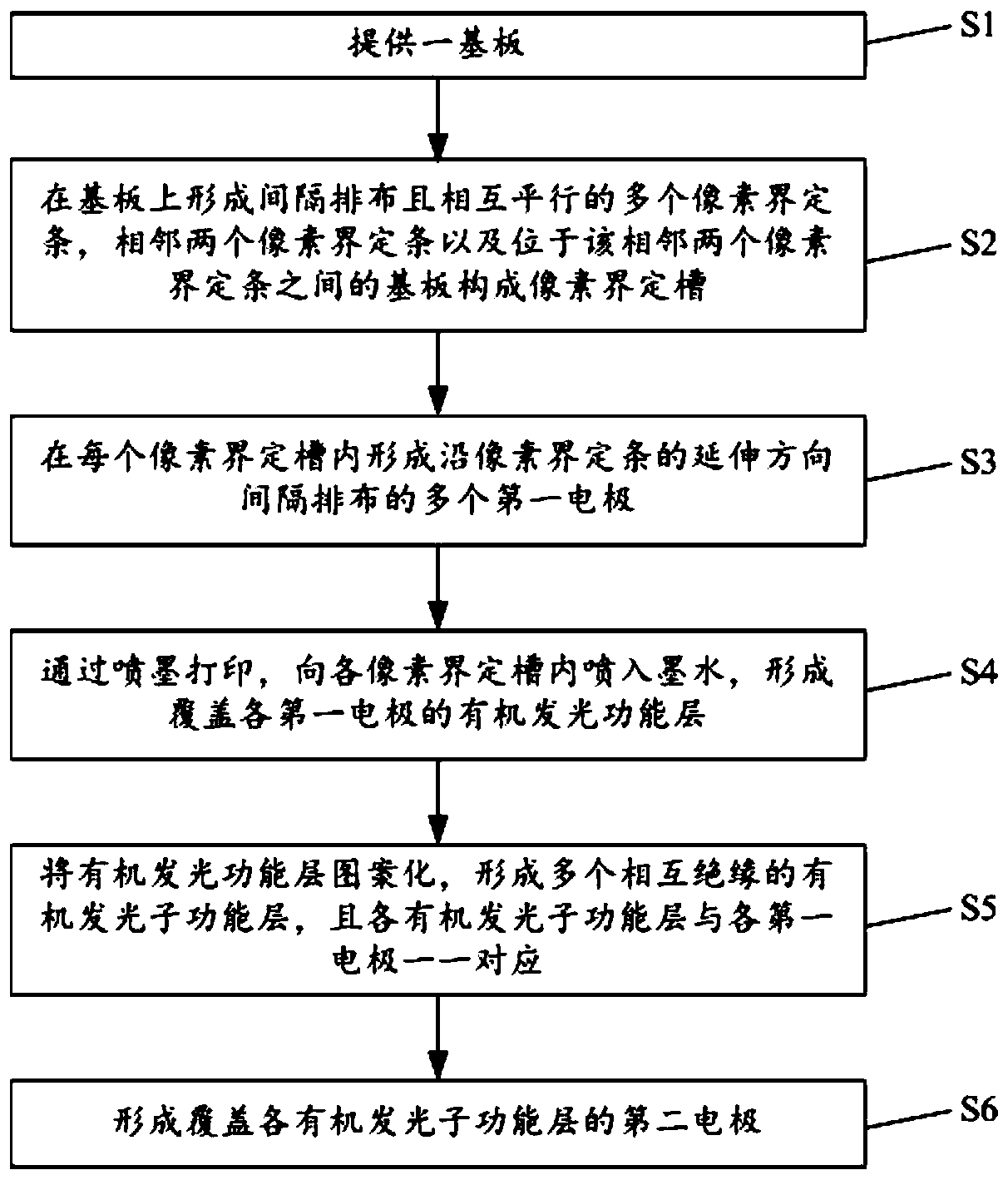
[0047] An embodiment of the present invention provides a method for manufacturing an organic light emitting diode display panel, such as image 3 As shown, the manufacturing method of the organic light emitting diode display panel includes:

[0048]Step S1, providing a substrate; the substrate may be a TFT array substrate, or other transparent substrates.

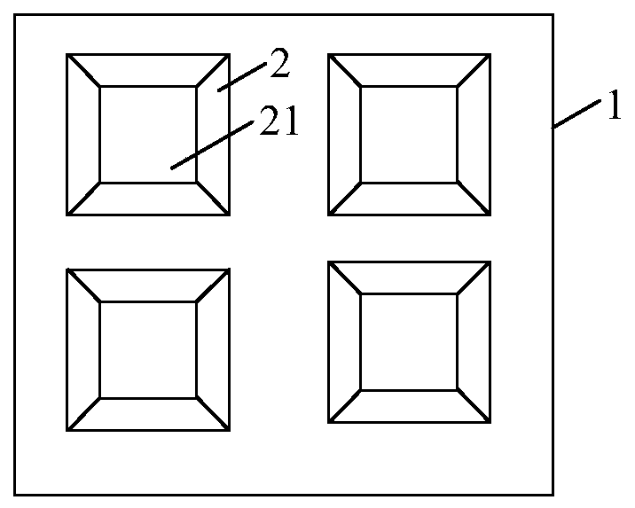
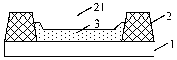
[0049] Step S2 , forming a plurality of pixel-defining strips arranged at intervals and pa...


PUM


Abstract

The invention discloses an organic light emitting diode display panel and a manufacturing method thereof, relates to the field of display technology, and solves the problem that the organic light emitting diode display panel is affected by the uneven thickness of the organic light emitting functional layer in the existing organic light emitting diode display panel. Technical problems with the display effect. The manufacturing method of the organic light emitting diode display panel includes: forming a plurality of pixel defining strips on the substrate, two adjacent pixel defining strips and the substrate between the adjacent two pixel defining strips forming a pixel defining groove; A plurality of first electrodes are formed in the pixel defining groove; ink is sprayed into each pixel defining groove by inkjet printing to form an organic light-emitting functional layer; the organic light-emitting functional layer is patterned to form a plurality of mutually insulated organic light-emitting sub-functional layers ; forming a second electrode covering each organic light-emitting sub-functional layer. The manufacturing method of the organic light emitting diode display panel provided by the present invention is applied to manufacturing the organic light emitting diode display panel.

Description

technical field [0001] The invention relates to the field of display technology, in particular to an organic light emitting diode display panel and a manufacturing method thereof. Background technique [0002] Compared with traditional liquid crystal display panels, organic light-emitting diode display panels have gradually become mainstream applications in the display field due to their advantages such as high brightness, wide viewing angle, low power consumption, and thin thickness. An organic light emitting diode in an existing organic light emitting diode display panel generally includes: a first electrode stacked on an array substrate, an organic light emitting functional layer and a second electrode. [0003] At present, the above-mentioned organic light-emitting functional layer is usually made by using an inkjet printing process, specifically, such as figure 1 and figure 2 As shown, firstly, a pixel defining layer 2 is formed on the substrate 1 on which the first ...

Claims


Application Information

Patent Timeline
Patent Type & Authority Patents(China)
IPC IPC(8): H01L27/32H01L51/52H01L51/56
CPCH10K71/135H10K59/122H10K50/813H10K71/00H10K50/15H10K50/16H10K50/81H10K50/82H10K50/171H10K99/00
Inventor 崔颖
Owner BOE TECH GRP CO LTD
Why Eureka
Try Eureka