SIP packaging structure with integrated photoelectric transceiver function and manufacturing method thereof

A technology of optoelectronic transceiver and packaging structure, applied in the coupling of optical waveguides, etc., can solve the problems of poor resistance to external force, low production efficiency, and many processes, so as to enhance the ability to resist external force, improve production efficiency, and avoid water vapor corrosion. Effect

Active Publication Date: 2019-08-23
JCET GROUP CO LTD
View PDF3 Cites 3 Cited by
  • Summary
  • Abstract
  • Description
  • Claims
  • Application Information

AI Technical Summary

Problems solved by technology

To complete a complete photoelectric transceiver module structure, it needs to be assembled one by one. The whole process has many procedures and the production efficiency is relatively low, and the anti-external force ability of the assembled photoelectric transceiver module structure is relatively poor. The assembled photoelectric transceiver module structure The airtightness is not good enough, and it is easy to be corroded by water vapor.

Method used


Image

  • SIP packaging structure with integrated photoelectric transceiver function and manufacturing method thereof
  • SIP packaging structure with integrated photoelectric transceiver function and manufacturing method thereof
  • SIP packaging structure with integrated photoelectric transceiver function and manufacturing method thereof

Examples


Embodiment Construction

[0046] The present invention will be further described in detail below in conjunction with the accompanying drawings and embodiments.

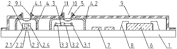
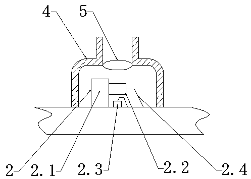
[0047] Such as figure 2 , image 3 As shown, a SiP packaging structure with integrated photoelectric transceiver function in this embodiment includes a substrate 1 on which an optical transmitter 2 and an optical receiver 3 are mounted, and the optical transmitter 2 includes a first A copper block 2.1, a laser 2.2 is mounted on the side of the first copper block 2.1, a backlight tube 2.3 is mounted on the substrate 1 below the laser 2.2, and the backlight tube 2.3 and the laser 2.2 are connected by a first metal wire 2.4 To the substrate 1, the optical receiver 3 includes a second copper block 3.1, a detector 3.2 and a pre-amplifier IC3.3 are mounted on the second copper block 3.1, and the connection between the detector 3.2 and the pre-amplifier IC3.3 between the detector 3.2 and the second copper block 3.1, and between the preamplifier IC...


PUM


Abstract

The invention relates to an SIP (session initiation protocol) packaging structure with the integrated photoelectric transceiving function and a process method thereof. The structure comprises a substrate (1). An optical transmitter (2) and an optical receiver (3) are attached to the substrate (1). A metal shell (4) is arranged outside the optical transmitter (2) and the optical receiver (3). A lens (5) is arranged inside the metal shell (4). A chip (6) and a passive device (7) are attached to the outer surface of the metal shell (4). The metal shell (4), the chip (6) and the passive device (7) are externally provided with a metal cover (9). The upper end of the upper hollow cylinder (4.1) of the metal shell (4) is exposed out of the metal cover to form a light opening (10). According to the invention, by adopting a metal shell component, a photoelectric sending module and a receiving module are integrated in an SIP (session initiation protocol) package. Therefore, the complex process of an existing product is simplified. The production efficiency is improved. Meanwhile, the external force resistance and the leakproofness of the product are improved.

Description

technical field [0001] The invention relates to a SiP packaging structure with an integrated photoelectric transceiver function and a manufacturing method thereof, belonging to the technical field of semiconductor packaging. Background technique [0002] Optical fiber technology has become more and more popular, and photoelectric modules have been widely used. The current photoelectric module is mainly assembled by receiving optical sub-assembly, transmitting optical sub-assembly, optical interface, internal circuit board, heat conducting frame and shell (see figure 1 ). Among them, the sending optical subassembly is to assemble the optical sending device on the sending side PCB. The optical sending device is generally composed of a laser (laser diode), a backlight tube (backlight detection tube), a thermistor, a TEC cooler, and an optical alignment mechanism, etc. The components are integrated inside a metal shell; the receiving optical subassembly is to assemble the ligh...

Claims


Application Information

Patent Timeline
Patent Type & Authority Patents(China)
IPC IPC(8): G02B6/42
Inventor 顾骁任慧
Owner JCET GROUP CO LTD
Why Eureka
Try Eureka