Pixel device, driving method used for same, and display device

The technology of a pixel and a driving unit is applied in the driving method of a pixel device and the field of a display device, and can solve problems such as long settling time, current-limited pixel circuit application, circuit structure or/and complex driving signal, etc., and achieve simple peripheral circuits, The effect of scanline reduction

Active Publication Date: 2017-12-01
PEKING UNIV SHENZHEN GRADUATE SCHOOL
View PDF11 Cites 7 Cited by
  • Summary
  • Abstract
  • Description
  • Claims
  • Application Information

AI Technical Summary

Problems solved by technology

The compensation accuracy of the current-type pixel circuit is relatively high, but it needs a relatively long settling time, especially in the case of low current and large parasitic capacitance on the data line
This severely limits the application of current-mode pixel circu

Method used


Image

  • Pixel device, driving method used for same, and display device
  • Pixel device, driving method used for same, and display device
  • Pixel device, driving method used for same, and display device

Examples


Embodiment 1

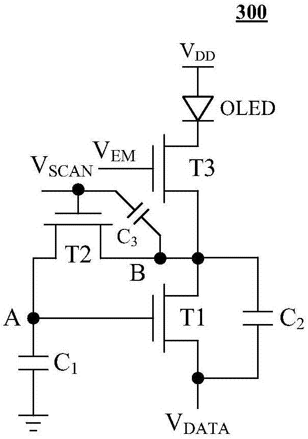
[0054] Please also see image 3 and Figure 4a ,in, image 3 It is a schematic diagram of the circuit structure according to the first embodiment of the present application, Figure 4a is a signal timing diagram according to the first embodiment of the present application. In this embodiment, each transistor is an N-type thin film transistor, and the active level at which each transistor is turned on is a high level. In addition, since a display device (such as a display) includes an array of a plurality of pixel devices, therefore, Figure 4a V in the timing SCAN[N] Corresponding to the scanning control signal received by the pixel device in the Nth row.

[0055] Such as image 3 As shown, the control electrode of the driving transistor T1 is coupled to the storage capacitor C1, the first electrode of the driving transistor T1 is coupled to the second electrode of the third transistor T3, and the second electrode of the driving transistor T1 is coupled to the data signa...

Embodiment 2

[0082] Figure 5 It is a schematic diagram of the circuit structure of the pixel device according to the second embodiment of the present application, Figure 6a is a signal timing diagram according to the second embodiment of the present application, Figure 6b is another signal timing diagram according to the second embodiment of the present application.

[0083] The difference from the above embodiments is that the light emitting device OLED is connected to the second electrode of the driving transistor T1 and the second power supply voltage V SS between. In addition, the second electrode of the second capacitor C2 is not coupled to the second electrode of the driving transistor T1. The first electrode of the third transistor T3 is coupled to the first supply voltage V DD .

[0084] Similar to Embodiment 1, the working process of the pixel device 500 shown in this embodiment is divided into four stages, namely initialization stage, threshold value extraction stage, dat...


PUM


Abstract

The invention discloses a pixel device, a driving method used for the pixel device, and a display device. The pixel device comprises a light emitting device, a light emitting control unit, a storage unit, and a driving unit. The light emitting control unit is configured to control whether the light emitting device gives out light responded to a light emitting control signal. The storage unit is configured to store threshold voltage information and write in data signals. The driving unit comprises a first transistor used to drive the light emitting device. The driving unit is coupled with the light emitting control unit and the storage unit, and is configured to extract threshold voltage information, and stores the threshold voltage information in the storage unit. The driving unit drives the light emitting device based on the stored threshold voltage information and the written in data signal. The threshold voltage information includes threshold voltage information of the first transistor. The pixel device can compensate threshold voltage drift of a drive transistor and the light emitting device.

Description

technical field [0001] The present application belongs to the field of display technology, and in particular relates to a pixel device capable of compensating changes in device threshold voltages, a driving method for the pixel device, and a display device. Background technique [0002] Due to the advantages of high brightness, high luminous efficiency, wide viewing angle and low power consumption, Organic Light-Emitting Diode (OLED) display has been extensively studied in recent years and has been rapidly applied to a new generation of displays. The OLED display can be driven in two ways: passive matrix OLED (PMOLED) and active matrix OLED (AMOLED). Although the cost of passive matrix driving is low, the required driving current is large, which will increase the degradation of OLED and reduce its service life. In addition, the passive matrix driving method has crosstalk and cannot achieve high-resolution display. In contrast, the active matrix driving method sets a differe...

Claims


Application Information

Patent Timeline
IPC IPC(8): G09G3/3233
CPCG09G3/3233
Inventor 张盛东王翠翠
Owner PEKING UNIV SHENZHEN GRADUATE SCHOOL
Why Eureka
Try Eureka