Vehicle lamp

A technology for lamps and vehicles, which is applied to headlights, vehicle parts, lighting and heating equipment, etc., and can solve the problems of limited number of semiconductor light-emitting elements, insufficient road illumination, and inability to use array light sources.

Active Publication Date: 2017-12-05
KOITO MFG CO LTD
View PDF11 Cites 15 Cited by
  • Summary
  • Abstract
  • Description
  • Claims
  • Application Information

AI Technical Summary

Problems solved by technology

[0009] However, in the lamp of Patent Document 2, since the projection lens is divided into upper and lower parts, there is room for improvement in the design of the appearance of the lamp when viewed from the front.
[0010] In addition, in the lamp of Patent Document 1, there is a portion where the light distribution patterns do not overlap each other near the boundary between the additional light distribution pattern for high beam and the light distribution pattern for low beam, and the road surface illumination may become insufficient.
[0011] In addition, in the lamp of Patent Document 1, there is a restriction on the number of semiconductor light emitting elements that can be mounted on the array light source in terms of the space of the lamp.
Therefore, it is sometimes impossible to form a light distribution pattern corresponding to the application and the situation by using an array light source

Method used


Image

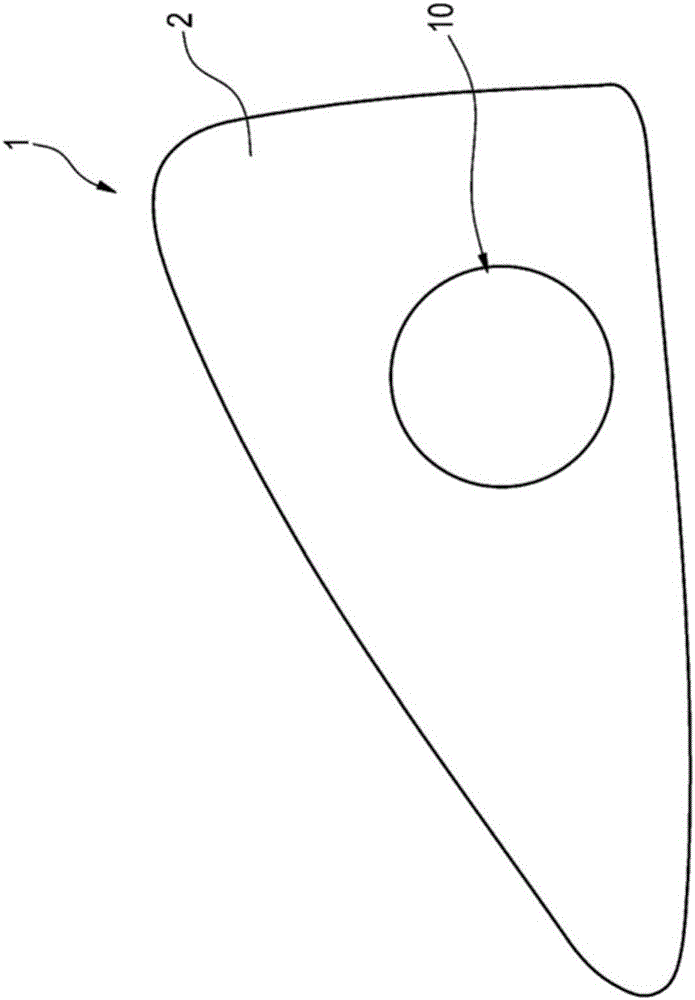
  • Vehicle lamp
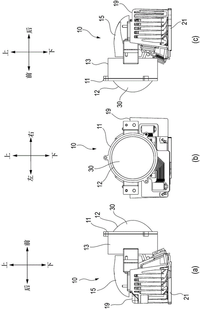
  • Vehicle lamp
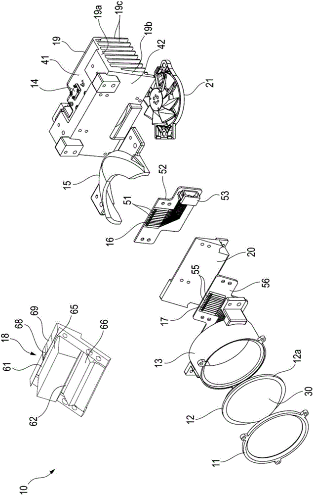
  • Vehicle lamp

Examples


Deformed example 1

[0329] Such as Figure 12 As shown, in Modification 1, one rigid substrate 70 is provided. The rigid substrate 70 is, for example, a glass epoxy substrate or a paper phenol substrate. The rigid substrate 70 is fixed and attached to the second surface 42 which is an inclined surface of the base member 19 . On this rigid substrate 70 , the first array light source 16 and the second array light source 17 are mounted vertically at intervals. A connector 71 is provided on one side of the rigid substrate 70 . A connector (not shown) of a power supply line is connected to the connector 71 , and power is supplied from the power supply line to the semiconductor light emitting element 51 of the first array light source 16 and the semiconductor light emitting element 55 of the second array light source 17 .

[0330] According to such a configuration, it is easy to arrange the first array light source 16 and the second array light source 17 at predetermined positions with respect to th...

Deformed example 2

[0332] Such as Figure 13 and Figure 14 As shown, in Modification 2, one flexible substrate 80 is provided. The flexible substrate 80 is, for example, a substrate in which a wiring pattern 82 made of copper foil is formed on a highly flexible base 81 made of a plastic film such as polyimide. The flexible substrate 80 is fixed and mounted on the second surface 42 which is an inclined surface of the base member 19 . On this flexible substrate 80 , the first array light source 16 and the second array light source 17 are mounted vertically at intervals. On one side of the flexible substrate 80 , a lead-out portion 83 extends, and a connector 84 is provided on the lead-out portion 83 . A connector (not shown) of a power supply line is connected to the connector 84 , and power is supplied from the power supply line to the semiconductor light emitting elements 51 of the first array light source 16 and the semiconductor light emitting elements 55 of the second array light source 1...

Deformed example 3

[0337] Such as Figure 15 As shown, in Modification 3, there is a projection lens 90 in which the convex shape of the output surface is divided into upper and lower parts. Specifically, the projection lens 90 has a first lens portion 91 on the upper side and a second lens portion 92 on the lower side, and the first lens portion 91 and the second lens portion 92 are integrated. The first lens part 91 has a first incident surface 91a and a first output surface 91b, and the second lens part 92 has a second incident surface 92a and a second output surface 92b.

[0338] In Modification 3, the light L from the low beam light source 14 and the light LA1 from the first array light source 16 enter the first incident surface 91 a of the first lens portion 91 and are emitted from the first output surface 91 b. In addition, the light LA2 from the second array light source 17 enters the second incident surface 92 a of the second lens unit 92 and exits from the second exit surface 92 b.

...


PUM


Abstract

The invention provides a vehicle lamp capable of preventing a large size of a lamp and improving design freedom of distribution patterns added to a regulated distribution patther. The vehicle lamp comprises a projection lens (2), a predetermined light source (14) arranged at a rear of the projection lens (12) and configured to emit light for forming a predetermined light distribution pattern (P), a reflector (15) configured to reflect the light (l) emitted from the predetermined light source (14) towards a first back focus (F1) of the projection lens (12), a first array light source (16) arranged at the rear of the projection lens (12) and including a plurality of semiconductor light emitting elements (51) aligned in at least one row, and a second array light source (17) arranged at the rear of the projection lens (12) and including a plurality of semiconductor light emitting elements (55) aligned in at least one row. The first array light source (16) and the second array light source (17) are arranged in an upper-lower direction.

Description

technical field [0001] The present invention relates to lamps for vehicles. Background technique [0002] In recent years, development of a vehicle lamp having an array light source in which a plurality of semiconductor light emitting elements such as LEDs (Light Emitting Diodes) are arranged in a row has been progressing. [0003] Patent Document 1 discloses a vehicle lamp which is a projection-type optical system using a single projection lens and has an array light source. [0004] Patent Document 1: Japanese Patent Laid-Open No. 2016-039020 [0005] Patent Document 2: Japanese Patent Laid-Open No. 2011-175818 [0006] However, in the lamp of Patent Document 1, there is a restriction on the number of semiconductor light emitting elements that can be mounted in the array light source in terms of the space of the lamp. Therefore, it may not be possible to add a desired light distribution pattern using an array light source to a predetermined light distribution pattern su...

Claims


Application Information

Patent Timeline
Patent Type & Authority Applications(China)
IPC IPC(8): F21S8/10F21V19/00F21Y115/00F21Y115/10F21W101/02F21W101/10
CPCF21V19/001F21Y2115/10F21Y2115/00F21S41/192F21S41/143F21S41/147F21S41/255F21S41/265F21S41/321F21S41/43F21S41/663F21S45/47F21S45/435F21S41/153F21W2102/145F21W2102/13F21S41/148F21S41/365F21S41/27F21S41/332F21S41/151F21S41/00F21S41/338F21S41/25F21S41/285F21S41/30F21S41/10F21S41/20
Inventor 高田贤一北泽达磨山本照亮河合宏树花田旭
Owner KOITO MFG CO LTD
Why Eureka
Try Eureka