Organic light-emitting diode (OLED) display panel and display device

A technology for display panels and display areas, applied in semiconductor devices, electrical components, circuits, etc., can solve problems such as cracks, OLED device failure, and thin film encapsulation layer and substrate peeling, and achieves improved bending reliability and extended service life. Effect

Active Publication Date: 2017-12-12
WUHAN TIANMA MICRO ELECTRONICS CO LTD
View PDF10 Cites 23 Cited by
  • Summary
  • Abstract
  • Description
  • Claims
  • Application Information

AI Technical Summary

Problems solved by technology

[0004] The inventors of the present application found that in the process of implementing the present application, cracks will inevitably occur in the cutting area of ​​the array substrate during the subsequent cutting process of the OLED display panel; when the OLED display panel is applied to a flexible OLED display device or a curved OLED display During installation, the cracks on the array substrate will further expand during the curling or bending process, and the thin film encapsulation layer and the second dam have a large bending stress at the bend, so that the thin film encapsulation layer and the substrate are easily peeled off. Cause water vapor and oxygen to enter the OLED device along the gap, causing the OLED device to fail

Method used


Image

  • Organic light-emitting diode (OLED) display panel and display device
  • Organic light-emitting diode (OLED) display panel and display device
  • Organic light-emitting diode (OLED) display panel and display device

Examples


Embodiment Construction

[0050] In order to improve the bending reliability of the OLED display device and prolong the service life of the OLED display device, an embodiment of the present invention provides an OLED display panel and a display device. In order to make the purpose, technical solution and advantages of the present invention clearer, the following examples are given to further describe the present invention in detail.

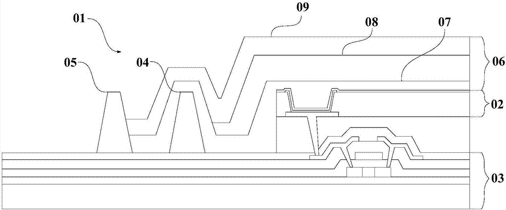
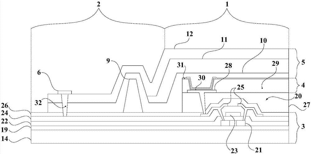
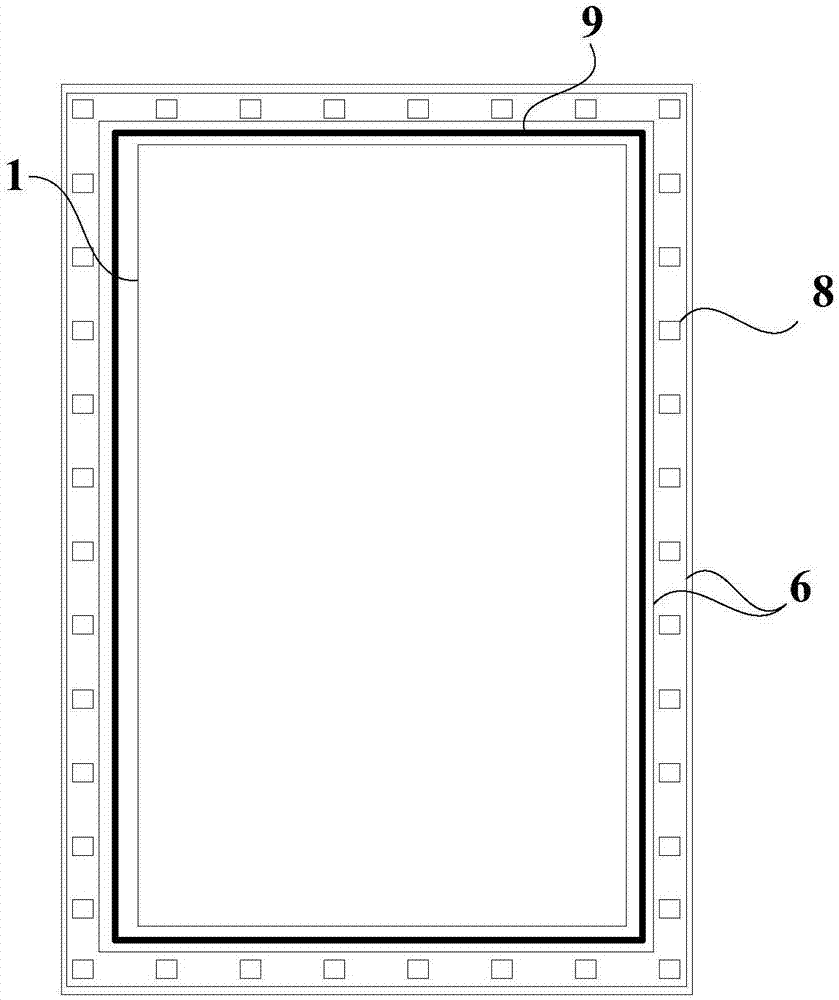
[0051] Such as figure 2 As shown, the embodiment of the present invention provides an OLED display panel, including a display area 1 and a peripheral area 2 outside the display area 1. The OLED display panel includes an array substrate 3, a light emitting unit 4 and The thin film encapsulation layer 5 , and the nail wall structure 6 disposed on the peripheral area 2 , wherein: the nail wall structure 6 penetrates the thin film encapsulation layer 5 and enters the array substrate 3 .

[0052]In the OLED display panel of the embodiment of the present invention, the light ...


PUM


Abstract

The invention discloses an organic light-emitting diode (OLED) display panel and a display device. The OLED display panel is used for improving the bending reliability of the OLED display device and prolonging the service lifetime of the OLED display device. The OLED display panel comprises a display region and a surrounding region, wherein the surrounding region is arranged outside the display region, the OLED display panel comprises an array substrate, a light-emitting unit, a thin film package layer and a nailed wall structure, the light-emitting unit and the thin film package layer are sequentially arranged on the array substrate, and the nailed wall structure is arranged on the surrounding region, penetrates through the thin film package layer and enters the array substrate.

Description

technical field [0001] The present invention relates to the field of display technology, in particular to an OLED (Organic Light-Emitting Diode, OLED for short) display panel and a display device. Background technique [0002] OLED display device, due to its thinness, lightness, wide viewing angle, active light emission, continuously adjustable light color, low cost, fast response speed, low energy consumption, low driving voltage, wide operating temperature range, simple production process, high luminous efficiency and Flexible display and other advantages have been listed as a promising next-generation display technology. [0003] At present, the display panel 01 of the OLED display device (the cross-sectional structure is as follows figure 1 (shown) during fabrication, the OLED device 02 is generally encapsulated by TFE (Thin Film Encapsulation, TFE for short) technology. The specific process steps are as follows: a first dam 04 and a second dam 05 are formed around the...

Claims


Application Information

Patent Timeline
Patent Type & Authority Applications(China)
IPC IPC(8): H01L27/32H01L51/52
CPCH10K59/12H10K50/8428
Inventor 刘雪宁李针英
Owner WUHAN TIANMA MICRO ELECTRONICS CO LTD
Why Eureka
Try Eureka