Flexible organic light emitting diode display and manufacturing method thereof

A technology for light-emitting diodes and a manufacturing method, which is applied in the fields of organic semiconductor devices, semiconductor/solid-state device manufacturing, photovoltaic power generation, etc., can solve the problems of limiting the application range and bending method of flexible OLED screens, uneven screen stress, etc., to improve the peeling phenomenon. , Improve the contact area, good compatibility

Inactive Publication Date: 2018-12-21
WUHAN CHINA STAR OPTOELECTRONICS SEMICON DISPLAY TECH CO LTD
View PDF3 Cites 0 Cited by
  • Summary
  • Abstract
  • Description
  • Claims
  • Application Information

AI Technical Summary

Problems solved by technology

When the flexible OLED screen is subjected to external shocks, or multiple bending / curling processes / laser lift-off (LLO), the inside of the screen is easily subject to uneven stress, and local peeling (peeling) occurs in the OLED light-emitting layer, such as figure 1 As mentioned, even whole screen peeling issues like figure 2 As mentioned, this greatly limits the scope and bending methods of flexible OLED screens

Method used


Image

  • Flexible organic light emitting diode display and manufacturing method thereof
  • Flexible organic light emitting diode display and manufacturing method thereof
  • Flexible organic light emitting diode display and manufacturing method thereof

Examples


Embodiment 1

[0048] In Embodiment 1, a method for manufacturing a flexible organic light emitting diode display 1 is provided, the method comprising:

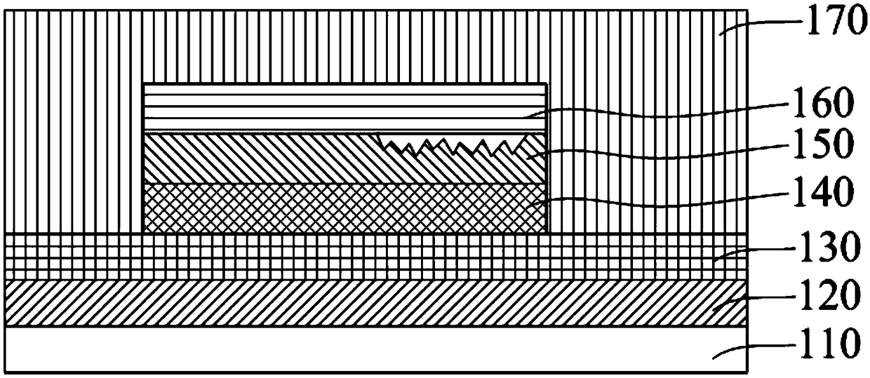
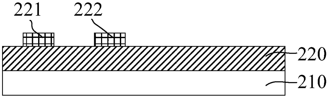
[0049] Step S10: forming an active array layer 220 on a flexible substrate 210, wherein a gate (not shown), a source 221 and a drain 222 are formed on the active array layer 220;

[0050] Step S20: forming a planarization layer 230 on the active array layer 220;

[0051] Step S30: performing photoetching on the planarization layer 230, so that at least a part of an upper surface of the planarization layer 230 forms an uneven surface 231;

[0052] Step S40: forming an anode layer 240 on the uneven surface 231 of the planarization layer 230;

[0053] Step S50: forming an organic light emitting display layer 250 on the anode layer 240;

[0054] Step S60: forming a cathode layer 260 on the organic light emitting display layer 250;

[0055] Step S70 : forming a protective layer 270 on the cathode layer 260 and the planarization layer 230 to c...

Embodiment 2

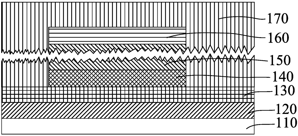
[0077] In Embodiment 2, a method for manufacturing a flexible organic light emitting diode display 1 is provided. The manufacturing method of embodiment 2 is substantially the same as that of embodiment 1, the only difference is that in step S30, it is implemented in step S32: the planarization layer is photoetched, so that a part of the planarization layer The entirety of the upper surface forms the uneven surface, such as Figure 10 shown.

[0078] More precisely, in this embodiment, step S30 includes step S32 and step S33: performing photoetching on the planarization layer 230, for example, through a photolithography process or ashing process (ashing) of the planarization layer, so that the All of an upper surface of the planarization layer forms the uneven surface 231, and at the same time, a through hole 234 is defined on the pair of the planarization layers, and the through hole penetrates the planarization layer 230 to reach the source 221 or the drain 222 . exist ...

Embodiment 3

[0080] Embodiment 3 provides a flexible OLED display 1 .

[0081] Figure 13 It is a side view of a flexible OLED display 1 according to the same embodiment of the present invention.

[0082] Such as Figure 13 As shown, the flexible organic light emitting diode display 1 includes:

[0083] a flexible substrate 210;

[0084] An active array layer 220, disposed on the flexible substrate 210, wherein the active array layer 210 includes a gate (not shown), a source 221 and a drain 222;

[0085] A planarization layer 230, disposed on the active array layer 220, wherein at least a part of an upper surface of the planarization layer 230 forms a first uneven surface 231, and a through hole 234 is defined in the In the planarization layer 230, wherein the via hole 234 penetrates the planarization layer 230 to reach the source electrode 221 or the drain electrode 222;

[0086] an anode layer 240 disposed on the first uneven surface 231 of the planarization layer, wherein an upper ...


PUM


Abstract

A method for fabricating a flexible organic light emitting diode display is provided. The fabrication method comprises the following steps: forming an active array layer on a flexible substrate; Forming a planarization layer on the active array layer; Photoetching the planarization layer such that at least a portion of an upper surface of the planarization layer forms an uneven surface; Forming ananode layer on an uneven surface of the planarization layer; Forming an organic light emitting display layer on the anode; Forming a cathode layer on the organic light emitting display layer; A protective layer is formed on the cathode layer and the planarization layer to cover the cathode layer and the planarization layer.

Description

technical field [0001] It relates to the technical field of displays, in particular to a flexible organic light emitting diode display and a manufacturing method thereof. Background technique [0002] With the development of display technology, although thin film transistor liquid crystal display (TFT-LCD) technology still dominates the mainstream display market, the development of a new generation of display technology for organic light-emitting diodes (OLED) and Applied in full swing and gradually being applied to many fields, such as wearable devices such as smart bracelets, smart watches, VR (Virtual Reality, that is, virtual reality) equipment, mobile phones, e-books, e-newspapers, televisions, personal Laptops, etc. [0003] Compared with traditional TFT-LCD technology, the biggest advantage of OLED is that it can be made into foldable / rollable products. When the flexible OLED screen is subjected to external shocks, or multiple bending / curling processes / laser lift-of...

Claims


Application Information

Patent Timeline
Patent Type & Authority Applications(China)
IPC IPC(8): H01L27/32H01L51/56H01L21/77
CPCH10K59/12H10K59/1201H10K71/00Y02E10/549H10K59/352H10K59/353H10K59/123H10K59/124H10K77/111H10K50/844H10K2102/311
Inventor 邬可荣崔昇圭
Owner WUHAN CHINA STAR OPTOELECTRONICS SEMICON DISPLAY TECH CO LTD
Why Eureka
Try Eureka