Method for hollowing copper foil at position of differential pair via hole

A differential and copper foil technology, applied in the field of PCB design, can solve the problems of heavy copper foil workload, etc., and achieve the effect of reducing workload, wide application prospects, and simple structure

Inactive Publication Date: 2017-12-12
ZHENGZHOU YUNHAI INFORMATION TECH CO LTD
View PDF4 Cites 8 Cited by
  • Summary
  • Abstract
  • Description
  • Claims
  • Application Information

AI Technical Summary

Problems solved by technology

[0004] The purpose of the present invention is to provide a method for hollowing out the copper foil at the via hole of the differential pair in order to solve the above technical problem

Method used


Image

  • Method for hollowing copper foil at position of differential pair via hole
  • Method for hollowing copper foil at position of differential pair via hole
  • Method for hollowing copper foil at position of differential pair via hole

Examples


Embodiment 1

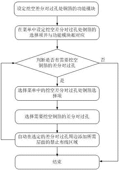
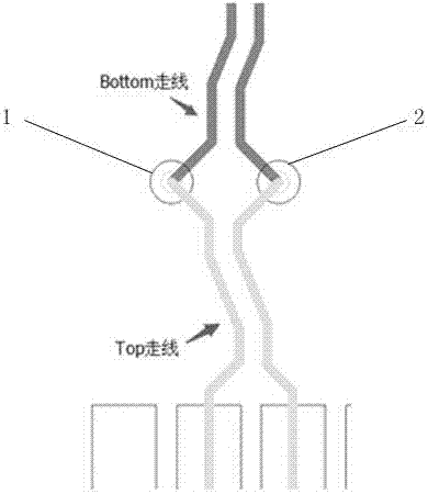
[0053] Example 1 image 3 As shown, it is necessary to hollow out the copper foil of the first differential pair positive signal via 1 and the first differential pair negative signal via 2 at the corresponding positions of the other PCB wiring layers outside the differential pair wiring layer;

[0054] Such as Figure 8 As shown, select the menu option "void for Diff via" to hollow out the copper foil at the differential pair via, click the differential pair via that needs to be hollowed out, and hollow out the first differential pair signal via 1 and No. A differential pair negative signal via 2 is a copper foil at the required level;

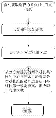
[0055] Automatically obtain the information of the differential pair via;

[0056] Automatically obtain the trace layer of the first differential pair positive signal via 1 and the first differential pair negative signal via 2, such as image 3 As shown, the positive signal of the first differential pair and the negative signal of the first differen...


PUM


Abstract

The invention provides a method for hollowing a copper foil at the position of a differential pair via hole. In the design process of a PCB, before the step of copper paving, the method comprises the following steps: step one, setting a functional module for hollowing the copper foil at the position of the differential pair via hole; step two, setting an option for hollowing the copper foil at the position of the differential pair via hole in a menu, and enabling the option to correspond to the functional module in the step one; step three, judging whether the differential pair via hole of the copper foil needs to be hollowed, if the differential pair via hole of the copper foil needs to be hollowed, selecting an option of the copper foil at the position of the differential pair via hole in the menu, entering into step four; if the differential pair via hole of the copper foil does not need to be hollowed, entering into step six; step four, selecting the differential pair via hole of the copper foil needing to be hollowed; step five, automatically adding a wiring forbidden area of a required layer surface on the periphery of the selected differential pair via hole; returning to step three; and step six, ending. The copper foil at the position of the differential pair via hole can be hollowed with one key, so that the Layout design efficiency is improved, and the workload of manual operation of Layout engineers is reduced.

Description

Technical field [0001] The invention belongs to the field of PCB design, and particularly relates to a method for hollowing out the copper foil at the via hole of a differential pair. Background technique [0002] In the PCB design stage of the server board, in order to ensure the same impedance before and after the high-speed signal line vias, the copper foil at the vias of the differential pair should be hollowed out in the design. Usually required. To manually check the size of the copper ring of the vias, add a forbidden routing area at other levels except for the differential pair wiring in the area composed of the vias, resulting in a large workload for the layout engineer and low design efficiency. [0003] This is a shortcoming of the prior art. Therefore, it is very necessary to provide a method of hollowing out the copper foil at the via hole of the differential pair in view of the above-mentioned defect in the prior art. Summary of the invention [0004] The purpose of ...

Claims


Application Information

Patent Timeline
Patent Type & Authority Applications(China)
IPC IPC(8): H05K3/00
CPCH05K3/0002H05K3/0005H05K2201/0784
Inventor 毛晓彤
Owner ZHENGZHOU YUNHAI INFORMATION TECH CO LTD
Why Eureka
Try Eureka