Storage, forming method thereof and semiconductor device

A memory and device technology, applied in the direction of semiconductor devices, semiconductor/solid-state device manufacturing, electric solid-state devices, etc., can solve the problems of unfavorable memory size reduction, the influence of capacitor capacitance, and the arrangement method cannot reach the density of capacitor arrangement.

Active Publication Date: 2017-12-15
CHANGXIN MEMORY TECH INC
View PDF3 Cites 10 Cited by
  • Summary
  • Abstract
  • Description
  • Claims
  • Application Information

AI Technical Summary

Problems solved by technology

With the continuous reduction of the size of semiconductor devices, the arrangement of regular square arrays can no longer achieve sufficient density of capacitors, which is not conducive to the reduction of memory size. the capacitance of the

Method used


Image

  • Storage, forming method thereof and semiconductor device
  • Storage, forming method thereof and semiconductor device
  • Storage, forming method thereof and semiconductor device

Examples


Embodiment 1

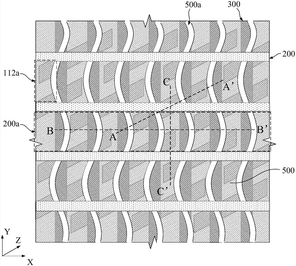
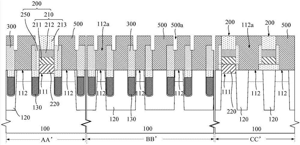
[0092] Figure 1ais a top view of the memory in Embodiment 1 of the present invention, Figure 1b for Figure 1a Shown is a schematic cross-sectional view of the memory in Embodiment 1 of the present invention along the directions AA', BB' and CC'.

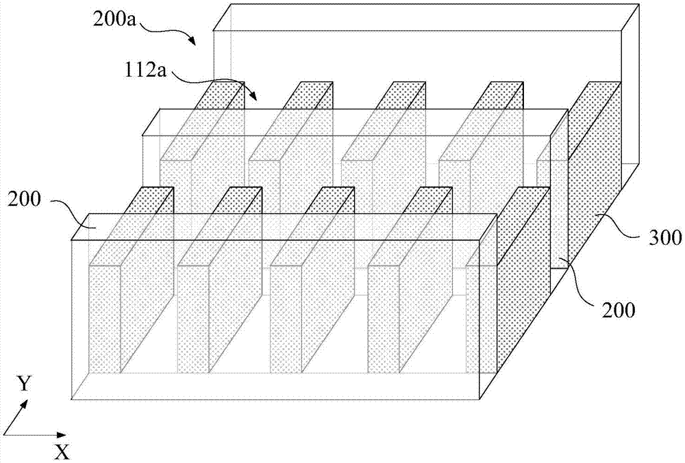
[0093] combine Figure 1a and Figure 1b As shown, the memory includes: a substrate 100 , a plurality of first isolation barriers 200 formed by bit lines 210 , a plurality of second isolation barriers 300 and a plurality of node contacts 500 .

[0094] Wherein, a plurality of active regions 110 are formed on the substrate 100, and one end of each active region 110 includes a node contact region 112, and the node contact regions 112 are connected to each other through the node contact 400. to a storage capacitor (not shown).

[0095] continue to refer Figure 1a As shown, in this embodiment, a plurality of node contact regions 112 are formed in one active region 110, and a bit line contact region 111 is also formed in the active ...

Embodiment 2

[0111] The present invention also provides a method for forming a memory, the forming method can form a plurality of node contacts staggered along the extension direction of the bit line as described above, which is beneficial to increase the electrode surface area of ​​the subsequently formed capacitor, Or the denseness of capacitor arrangement can be increased without changing the electrode surface area of ​​the capacitor.

[0112] figure 2 It is a schematic flow chart of the method for forming a capacitor in Embodiment 2 of the present invention, as figure 2 As shown, the forming method of the capacitor includes:

[0113] Step S110, providing a substrate, in which a plurality of active regions are formed, and one end of each active region includes a node contact region;

[0114] Step S120, forming a plurality of bit lines on the substrate, the bit lines extending along the first direction are mainly used to form a plurality of first isolation barriers, and the distance ...

Embodiment 3

[0182] In a semiconductor device, a conductive contact is usually used to lead out the contact area and realize electrical connection with other components formed subsequently. In small-sized semiconductor devices, the components above the conductive contacts can be densely arranged in order to realize the subsequent formation. At this time, the distribution of the conductive contacts near the top can be adjusted to further improve the follow-up. The arrangement of the resulting components.

[0183] Specifically, the semiconductor device provided by the present invention includes:

[0184] a substrate having a plurality of contact regions formed therein;

[0185] A plurality of first isolation barriers are formed on the substrate and extend along a first direction, and the intervals between two adjacent first isolation barriers define an area extending along the first isolation barriers. the groove;

[0186] a plurality of second isolation barriers formed on the substrate a...


PUM


Abstract

The invention provides a storage, a forming method thereof and a semiconductor device. On the basis that a first isolation screen and a second isolation screen define a contact window, the top surface of the second isolation screen is lower than that of the first isolation screen, so that the space above the second isolation screen can be utilized, the node contact top can extend in the extension direction of the first isolation screen so that the the second isolation screen can be covered, further a plurality of nodes are arranged in a staggering manner on the upper surfaces of the connection surfaces of the nodes and capacitors, accordingly, the following capacitors can be arranged in the staggering manner, so that not only can the capacitance of the capacitors be improved, but also the dense degree of the capacitor arrangement can be further improved.

Description

technical field [0001] The invention relates to the technical field of semiconductors, in particular to a memory, a method for forming the same, and a semiconductor device. Background technique [0002] A memory typically includes a capacitor for storing an electrical charge representing stored information and a storage transistor connected to the storage element. An active region, a drain region and a gate are formed in the memory transistor, the gate is used to control the flow of current between the source region and the drain region, and is connected to a word line conductor, and the source region is used to form The bit line contact area is used to connect to the bit line, and the drain area is used to form a node contact area to be connected to the capacitor. [0003] In the manufacturing process of the memory, the storage transistor is usually formed first to prepare a node contact region, so that a node contact can be prepared on the node contact region, and the nod...

Claims


Application Information

Patent Timeline
Patent Type & Authority Applications(China)
IPC IPC(8): H01L27/108H01L21/8242
CPCH10B12/31H10B12/315H10B12/033H10B12/0335
Inventor 不公告发明人
Owner CHANGXIN MEMORY TECH INC
Why Eureka
Try Eureka