OLED display substrate and manufacturing method thereof, and OLED display device

A technology for display substrates and substrates, used in semiconductor/solid-state device manufacturing, organic semiconductor devices, electrical components, etc., can solve problems such as layer fracture or peeling, OLED device failure, etc., to reduce fracture or peeling and improve bending reliability. , the effect of prolonging the service life

Active Publication Date: 2017-12-15
BOE TECH GRP CO LTD
View PDF2 Cites 28 Cited by
  • Summary
  • Abstract
  • Description
  • Claims
  • Application Information

AI Technical Summary

Problems solved by technology

[0005] The inventors of the present application found in the process of implementing the present application that when the OLED display substrate is applied to a flexible OLED display device or a curved OLED display device, there is a large bending stress at the bend between the barrier wall 02 and the packaging structure layer, which is extremely It is easy to cause layer fracture or peeling, so that water vapor and oxygen enter the OLED device along the gap, causing the OLED device to fail

Method used


Image

  • OLED display substrate and manufacturing method thereof, and OLED display device
  • OLED display substrate and manufacturing method thereof, and OLED display device
  • OLED display substrate and manufacturing method thereof, and OLED display device

Examples


Embodiment Construction

[0057] In order to improve the bending reliability of the OLED display device and prolong the service life of the OLED display device, embodiments of the present invention provide an OLED display substrate, a manufacturing method thereof, and an OLED display device. In order to make the purpose, technical solution and advantages of the present invention clearer, the following examples are given to further describe the present invention in detail.

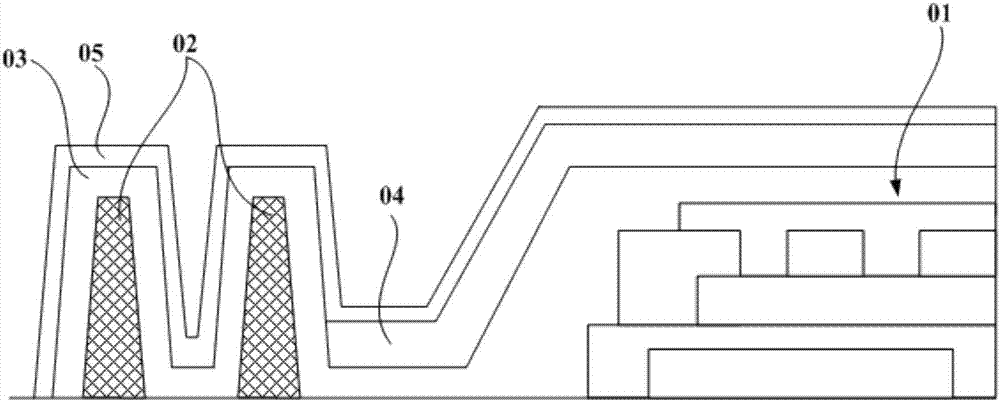
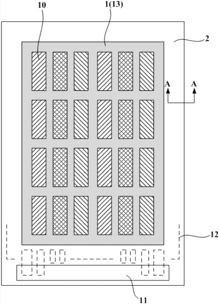
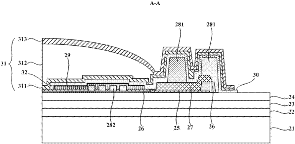
[0058] like figure 2 and image 3 As shown, the embodiment of the present invention provides an OLED display substrate, including a display area 1 and a non-display area 2 surrounding the display area 1. The OLED display substrate includes a retaining wall 281 arranged in the non-display area 2, and a And extend to the encapsulation structure layer 31 covering the barrier wall 281 , in addition, the OLED display substrate further includes a metal halide layer 30 located between the barrier wall 281 and the encapsulation structure ...


PUM


Abstract

The present invention discloses an OLED (Organic Light-Emitting Diode) display substrate and a manufacturing method thereof, and an OLED display device. The objective of the invention is to improve the bending reliability and prolong the service life of an OLED display device. The OLED display substrate comprises: a display area, a non-display area arranged around the display area, a retaining wall arranged at the non-display area, a packaging structure layer configured to cover the display area and extending to cover the retaining wall, and a metal halide layer located between the retaining wall and the packaging structure layer and configured to at least cover the retaining wall. The metal halide layer is increased between the retaining wall and the packaging structure layer, and the interface bonding force between the metal halide layer and the retaining wall and between the metal halide layer and the packaging structure layer is good to reduce the fracture or delamination of the edges of the OLED display substrate so as to effectively prevent steam and oxygen from entering the internal portion of the OLED display substrate for erosion of an OLED device and prolong the service life of the OLED display device.

Description

technical field [0001] The present invention relates to the field of display technology, in particular to an OLED (Organic Light-Emitting Diode, OLED for short) display substrate, a manufacturing method thereof, and an OLED display device. Background technique [0002] OLED display device, due to its thinness, lightness, wide viewing angle, active light emission, continuously adjustable light color, low cost, fast response speed, low energy consumption, low driving voltage, wide operating temperature range, simple production process, high luminous efficiency and Flexible display and other advantages have been listed as a promising next-generation display technology. [0003] Studies have shown that components such as water vapor and oxygen in the air have a great impact on the life of OLED devices in OLED display devices. This is because: OLED devices need to inject electrons from the cathode when they work, which requires the lower the cathode work function, the better, but...

Claims


Application Information

Patent Timeline
Patent Type & Authority Applications(China)
IPC IPC(8): H01L27/32H01L51/52H01L51/56
CPCH10K59/12H10K50/844H10K59/1201H10K71/00H10K59/35H10K50/8426H10K2102/00H10K59/131
Inventor 孙韬张嵩王有为王涛
Owner BOE TECH GRP CO LTD
Why Eureka
Try Eureka