Supercharge Your Innovation With Domain-Expert AI Agents!

Display substrate, manufacturing method thereof, and display device

A technology for display substrates and base substrates, which is applied in semiconductor devices, electrical components, circuits, etc., and can solve problems such as easy fracture and large stress

Active Publication Date: 2021-01-29
BOE TECH GRP CO LTD
View PDF6 Cites 0 Cited by
  • Summary
  • Abstract
  • Description
  • Claims
  • Application Information

AI Technical Summary

Problems solved by technology

[0005] However, in practical applications, it is found that since there is a climbing area at the junction of the bending-resistant area and the frame area corresponding to the signal wiring layer, when bending the non-display area, due to the climbing area corresponding to the signal wiring layer, a relatively large Large deformation, resulting in greater stress at this position, prone to fracture

Method used


Image

  • Display substrate, manufacturing method thereof, and display device
  • Display substrate, manufacturing method thereof, and display device
  • Display substrate, manufacturing method thereof, and display device

Examples


Embodiment 3

[0057] Embodiment 3 of the present invention provides a display device. The display device includes: a display substrate. The display substrate adopts the display substrate provided in Embodiment 1 or Embodiment 2 above. For details, please refer to Embodiment 1 and Embodiment 2 above. The content of the second is not repeated here.

[0058] The display device can be a product or component with a display function such as a television, a monitor, a tablet computer, a mobile phone, an electronic paper, a navigator, a digital photo frame, a video camera, a camera, and the like.

Embodiment 4

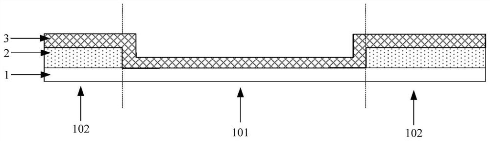
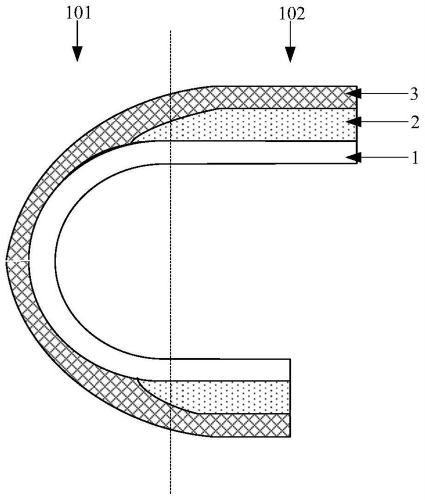
[0060] Figure 11 A flow chart of a method for preparing a display substrate provided in Embodiment 4 of the present invention, such as Figure 11 As shown, the preparation method is used to prepare the display substrates in the first and second embodiments above. The display substrate is divided into a display area and a non-display area surrounding the display area. A bending-resistant area and a frame area are set in the non-display area. The preparation method includes:

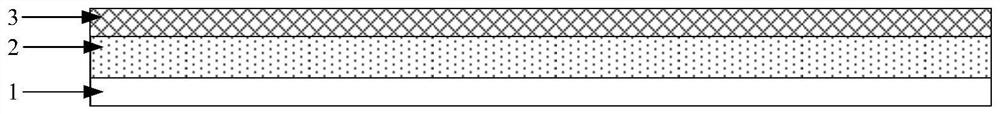
[0061] Step S1, forming an inorganic insulating layer on the base substrate at positions corresponding to the display area and the frame area.

[0062] Firstly, based on the existing thin film transistor technology, a whole-layer inorganic insulating layer is provided on the base substrate, and the inorganic insulating layer includes at least one of an inorganic buffer layer, a gate insulating layer, and an interlayer insulating layer. Then, the portion of the inorganic insulating layer corresponding to...


PUM


Abstract

The invention discloses a display substrate, a preparation method thereof, and a display device, comprising: a base substrate, an inorganic insulating layer is arranged on the base substrate corresponding to the display area and the frame area, and an inorganic insulating layer is arranged on the base substrate corresponding to the bending-resistant area. A first organic buffer layer is provided, the thickness of the first organic buffer layer is equal to the thickness of the organic insulating layer, a second organic buffer layer is provided on the side of the first organic buffer layer facing away from the base substrate, and the second organic buffer layer and the The bending-resistant area is provided correspondingly, and the side of the second organic buffer layer facing away from the base substrate is provided with a signal wiring layer. The technical solution of the present invention arranges the first organic buffer layer and the second organic buffer layer in the bending-resistant area, so that the signal wiring layer on the second organic buffer layer presents an "overall convex" state. When the non-display area When bending, the portion of the signal wiring layer corresponding to the bending-resistant area undergoes small deformation, thereby avoiding the problem of fracture of this portion due to excessive stress.

Description

technical field [0001] The invention relates to the field of display technology, in particular to a display substrate, a preparation method thereof, and a display device. Background technique [0002] A flexible display device is a display device formed based on a flexible base material. Since the flexible display device has the characteristics of rollability, wide viewing angle, and portability, the flexible display device has broad application prospects and good market potential in most display application fields such as portable products. [0003] figure 1 It is a schematic cross-sectional view of a non-display area of ​​a flexible display panel in the prior art; figure 1 As shown, the flexible display panel includes a display area 1a and a non-display area 1b surrounding the display area. In the non-display area 1b, there are inorganic insulating layers 2 on the upper layer and the lower layer of the signal wiring layer 3 (located on the back of the signal wiring layer...

Claims


Application Information

Patent Timeline
Patent Type & Authority Patents(China)
IPC IPC(8): H01L27/32
CPCH10K59/12H10K59/131
Inventor 蔡鹏陈立强宋平王有为
Owner BOE TECH GRP CO LTD
Features
  • R&D
  • Intellectual Property
  • Life Sciences
  • Materials
  • Tech Scout
  • Unparalleled Data Quality
  • Higher Quality Content
  • 60% Fewer Hallucinations
Learn More