Microwave device and assembly method thereof

A technology of microwave devices and assembly methods, which is applied in the direction of assembling printed circuits with electric components, electrical components, printed circuit parts, etc., can solve the problems of long design and processing cycle, low assembly efficiency, difficult assembly, etc., and achieve low cost, Simple assembly and high efficiency

Inactive Publication Date: 2017-12-15
THE 13TH RES INST OF CHINA ELECTRONICS TECH GRP CORP
View PDF5 Cites 4 Cited by
  • Summary
  • Abstract
  • Description
  • Claims
  • Application Information

AI Technical Summary

Problems solved by technology

For compact module and component-level products, especially in the millimeter wave field, the existing low-cost, mass-produced technical means are still lacking, or it is difficult to assemble and the assembly efficiency is low (gold-plated gaskets are used after digging grooves), or Expensive (LTCC), or long design and processing cycles (multilayer substrates)

Method used


Image

  • Microwave device and assembly method thereof
  • Microwave device and assembly method thereof
  • Microwave device and assembly method thereof

Examples


Embodiment Construction

[0025] The technical solutions in the embodiments of the present invention are clearly and completely described below in conjunction with the accompanying drawings in the embodiments of the present invention. Obviously, the described embodiments are only part of the embodiments of the present invention, not all of them. Based on the embodiments of the present invention, all other embodiments obtained by persons of ordinary skill in the art without making creative efforts belong to the protection scope of the present invention.

[0026] In the following description, a lot of specific details are set forth in order to fully understand the present invention, but the present invention can also be implemented in other ways different from those described here, and those skilled in the art can do it without departing from the meaning of the present invention. By analogy, the present invention is therefore not limited to the specific examples disclosed below.

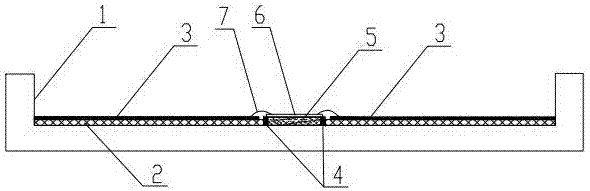
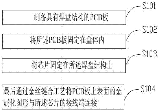
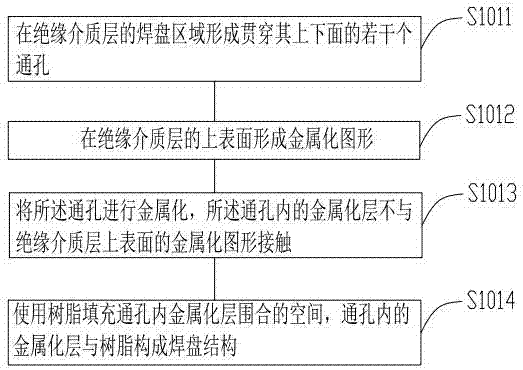
[0027] Such as figure ...


PUM


Abstract

The invention discloses a microwave device and an assembly method thereof, and relates to the technical field of electronic components. The microwave device comprises a box body, and is characterized in that the internal part of the box body is fixedly provided with a PCB, the surface, which is connected with the box body, of the PCB is provided with an insulating dielectric layer, the upper surface of the insulating dielectric layer is provided with a PCB pattern, the insulating dielectric layer is provided with a plurality of through holes penetrating the upper and lower surface of the insulating dielectric layer, the side wall of each through hole is provided with a metallized layer, the space enclosed by the metalized layer in each through hole is filled with resin, the metalized layer and the resin form a bonding pad structure, a chip is fixed at the upper surface of the bonding pad, the back surface of the chip is connected with the box body through the metalized layer, and a wiring terminal of the chip is connected with the PCB pattern through a gold bonding wire. The microwave device has the advantages of small spacing between strip lines, low cost, no stress transition, simple assembly and high efficiency.

Description

technical field [0001] The invention relates to the technical field of electronic components, in particular to a microwave device and an assembly method thereof. Background technique [0002] At present, in order to reduce production costs and improve manufacturability, electronic equipment and devices are developing towards multi-chip integration. Multi-chip assembly technology has higher and higher requirements for assembly process. For compact module and component-level products, especially in the millimeter wave field, the existing low-cost, mass-produced technical means are still lacking, or it is difficult to assemble and the assembly efficiency is low (gold-plated gaskets are used after digging grooves), or Expensive (LTCC), or long design and processing cycle (multilayer substrate). Contents of the invention [0003] The technical problem to be solved by the present invention is how to provide a microwave device with small stripline spacing, low cost, no need for...

Claims


Application Information

Patent Timeline
Patent Type & Authority Applications(China)
IPC IPC(8): H05K3/30H05K3/32H05K1/11
CPCH05K1/113H05K3/303H05K3/32H05K2201/10212
Inventor 肖宁徐达戈江娜郝金中王立发
Owner THE 13TH RES INST OF CHINA ELECTRONICS TECH GRP CORP
Why Eureka
Try Eureka